Structural material for modulation of terahertz waves
A structural material and terahertz technology, applied in the field of electronics, can solve problems such as application limitations and achieve the effect of large modulation depth
- Summary
- Abstract
- Description
- Claims
- Application Information
AI Technical Summary
Problems solved by technology
Method used
Image
Examples
Embodiment Construction
[0017] Taking the linear electromagnetic resonance unit as an example, the preparation, testing and analysis process of the structural material for terahertz wave modulation provided by the present invention is described in detail below:
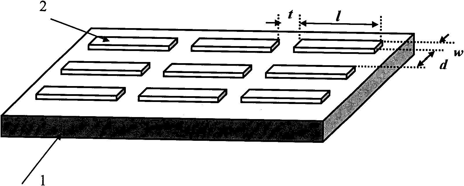
[0018] Step 1: Use the commercial software CST Microwave Studio to establish a structural material model structure for terahertz wave modulation, in which the electromagnetic resonator array 1 is an optimized linear electromagnetic resonator unit on the premise that the electromagnetic resonator unit material is a perfect metal The length l, width w, distance t and d between elements to obtain the maximum resonance depth. The best parameters obtained are: l=108 μm, w=13.5 μm, t=6 μm, d=30 μm.
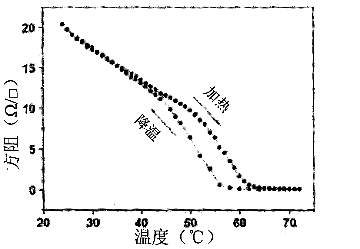
[0019] Step 2: Using radio frequency magnetron sputtering method, by VO 2 The target is deposited on a quartz glass substrate with an area of 10 mm × 10 mm and a thickness of 500 microns to deposit about 0.8 micron thick VO 2 film. figure 2 The ...
PUM
| Property | Measurement | Unit |
|---|---|---|
| Thickness | aaaaa | aaaaa |
| Thickness | aaaaa | aaaaa |
Abstract
Description
Claims
Application Information


