Micro-electromechanical device and method for fabricating the same

A micro-electromechanical and manufacturing method technology, which is applied in the direction of manufacturing micro-structure devices, micro-electronic micro-structure devices, circuits, etc., to achieve the effect of narrow gaps

Inactive Publication Date: 2011-01-12
SANYO ELECTRIC CO LTD
View PDF2 Cites 2 Cited by
  • Summary
  • Abstract
  • Description
  • Claims
  • Application Information

AI Technical Summary

Problems solved by technology

[0012] However, in conventional photolithography and etching groove processing, for example, when using an i-line exposure machine, forming a groove width of about 0.35 μm is the limit, and it is difficult to further reduce the size

Method used


Image

  • Micro-electromechanical device and method for fabricating the same
  • Micro-electromechanical device and method for fabricating the same
  • Micro-electromechanical device and method for fabricating the same

Examples


Embodiment Construction

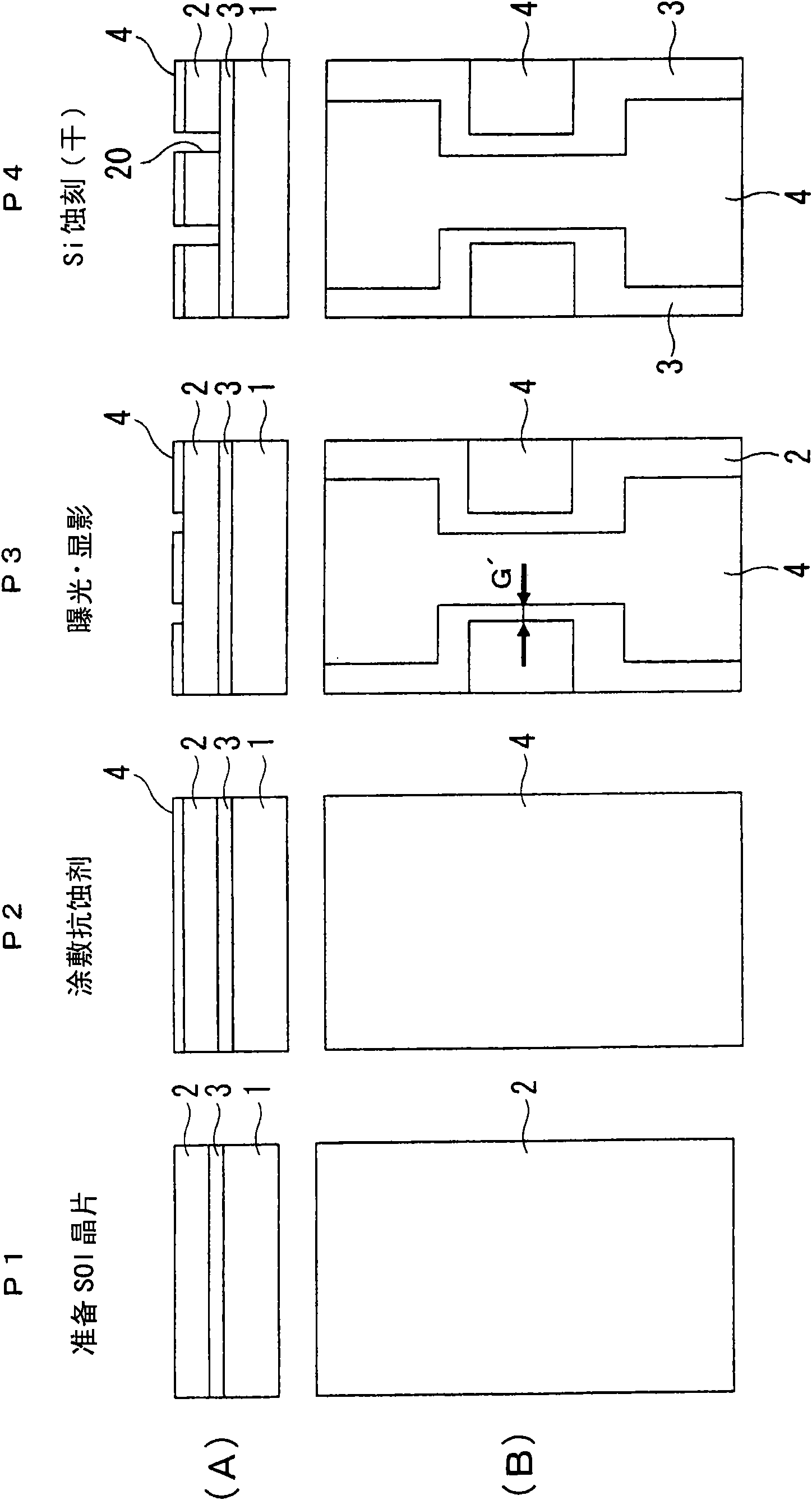
[0039] Below, with reference to the accompanying drawings, based on the Figure 6 The manner in which the MEMS resonator is shown is implemented to illustrate the invention.

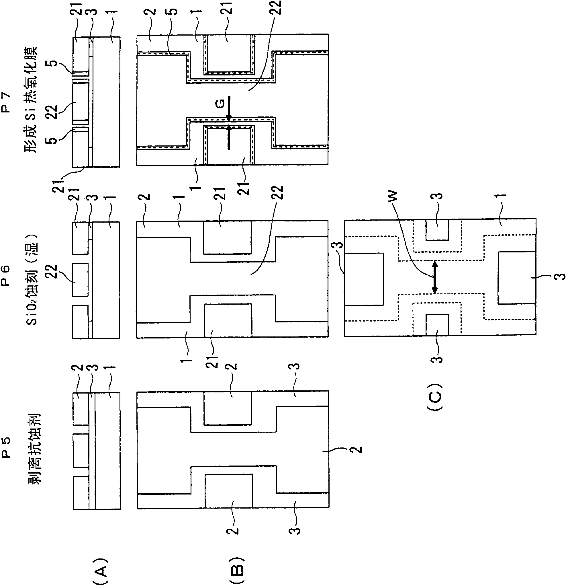
[0040] figure 1 and figure 2 Steps P1 to P7 for forming the resonator and the left and right electrodes of the MEMS resonator of the present invention are shown. In addition, in figure 1 and figure 2 Among them, (A) is a longitudinal sectional view, and (B) and (C) are top views.

[0041] First, in figure 1 In step P1 of , prepare to laminate SiO on the surface of Si layer 1 to be the substrate 2 layer 3 and Si layer 2 to form an SOI wafer.

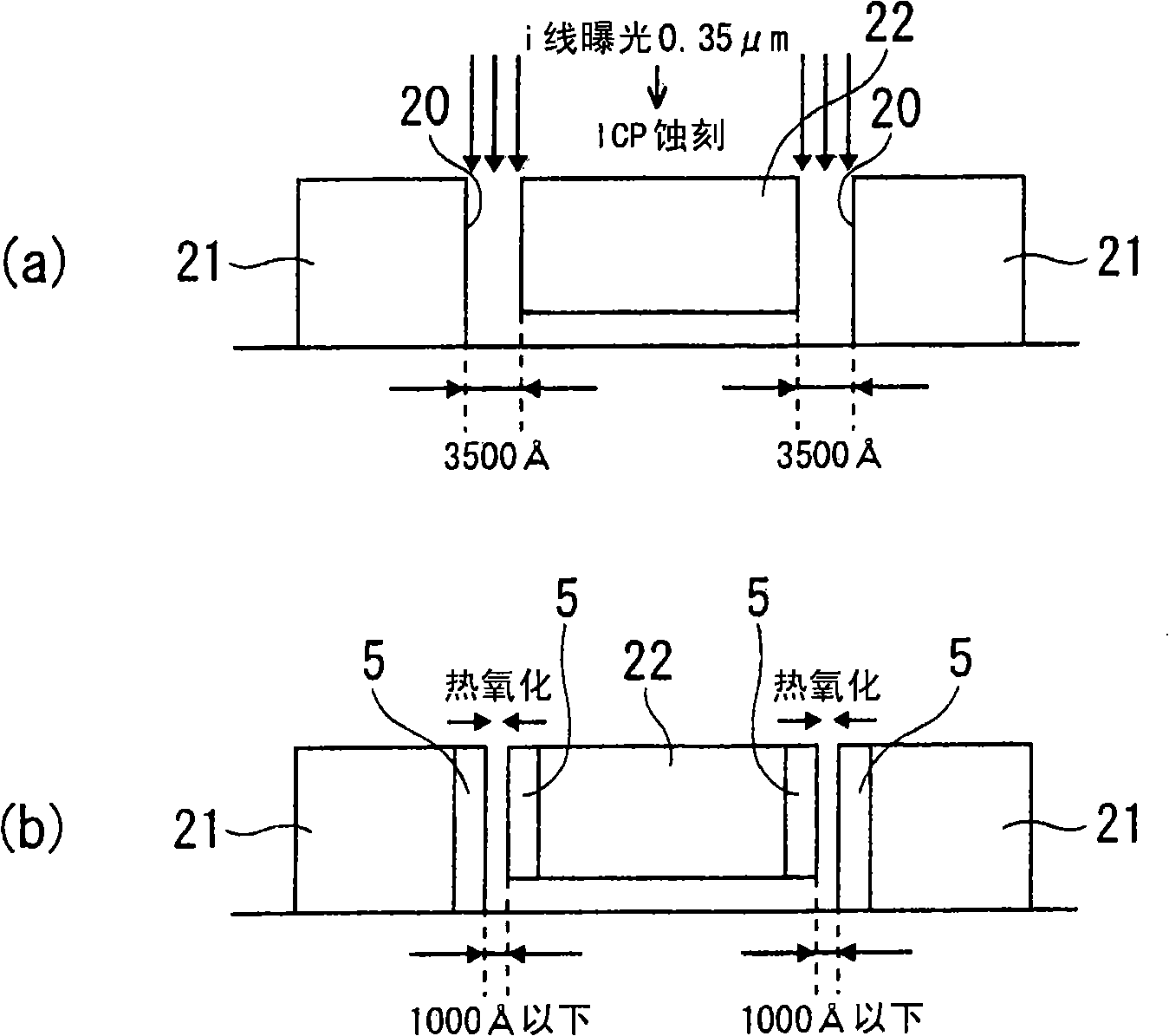
[0042] Next, in step P2 , resist 4 is applied to the surface of Si layer 2 . Then, in step P3, the resist 4 is exposed and developed using an i-line exposure machine to form a groove pattern having the gap G'. Here, the limit of the gap G' is 0.35 µm.

[0043] Next, in step P4 , dry etching is performed on the Si layer 2 to form the grooves 20 on the S...


PUM

PropertyMeasurementUnit
thicknessaaaaaaaaaa

Abstract

Provided is a structure of a microelectromechanical device wherein the gap can be made narrower. Also provided is a process for fabricating the microelectromechanical device. A microelectromechanical device comprises a resonator (22) and an electrode (21) facing each other, a pair of thermal oxide film (5, 5) formed on the surfaces of the resonator and electrode facing each other and a narrow gap provided between the thermal oxide films. A process for fabricating a microelectromechanical device comprises a step of processing an Si layer to be the resonator (22) and the electrode (21) by using photolithography and etching to form a trench (20) to be a gap, and a step of performing thermal oxidation on the Si layer to form a pair of thermal oxide films (5, 5) of Si on the opposite surfaces of the trench (20).

Description

technical field [0001] The invention relates to the structure and manufacturing method of micro-electromechanical devices such as micro-mechanical resonators and micro-mechanical capacitors manufactured by micro-processing technology in the field of semiconductors. Background technique [0002] In recent years, a so-called micro-electromechanical system (MEMS) technology in which a fine mechanical structure and a circuit are integrated using microfabrication technology in the semiconductor field has been developed, and efforts have been made to apply it to filters and resonators. [0003] Figure 6 A conventional micromechanical resonator using MEMS technology is shown (Non-Patent Document 1). In this micromechanical resonator, a resonator 90 is provided on a substrate 96 as shown in the figure. The support beams 91 to 91 are configured, and the base end portions of the respective support beams 91 are respectively fixed to the base plate 96 by anchors 93 . Thus, resonator ...

Claims


Application Information

Patent Timeline
Patent Type & Authority Applications(China)
IPC IPC(8): B81B3/00B81C1/00H01G5/16H03H3/007H03H9/24
CPCB81C1/00182H03H9/2463B81B2203/033B81B2203/0118B81C2201/0178H01G5/16B81B2203/04H03H2009/02496B81B2201/0271H03H3/0072Y10T29/49002
Inventor 长崎宽范
Owner SANYO ELECTRIC CO LTD
Why Eureka
Try Eureka