LED integrated light source board and manufacturing method thereof

A technology of LED light source and manufacturing method, which is applied in the direction of light source fixing, lighting device, lighting device cooling/heating device, etc., can solve the problems of the accuracy of lens light distribution, inconsistent optical center, expensive materials, etc., to avoid all Reflection phenomenon, simple manufacturing process, and the effect of improving luminous efficiency

Active Publication Date: 2011-01-19
NANKER GUANGZHOU SEMICON MFG
View PDF5 Cites 10 Cited by
  • Summary
  • Abstract
  • Description
  • Claims
  • Application Information

AI Technical Summary

Problems solved by technology

For the planar integrated LED light source, if a multi-chip LED module or a multi-chip LED integrated block is used as a light source unit, such as Figure 5 In the method shown, all the LED chips in the unit are covered by a lens, that is, a single lens with multiple chips is used. In order to cover all the LED chips, the radius of the single lens becomes very large, making the entire lens larger , the amount of material is large, because the material of the lens is optical silica gel or resin, which is expensive, which makes the cost of the lens high and uneconomical; and the single lens makes the optical center of each LED chip inconsistent, and the accuracy of the lens light distribution be affected to a certain extent

Method used


Image

  • LED integrated light source board and manufacturing method thereof
  • LED integrated light source board and manufacturing method thereof
  • LED integrated light source board and manufacturing method thereof

Examples


Embodiment 1

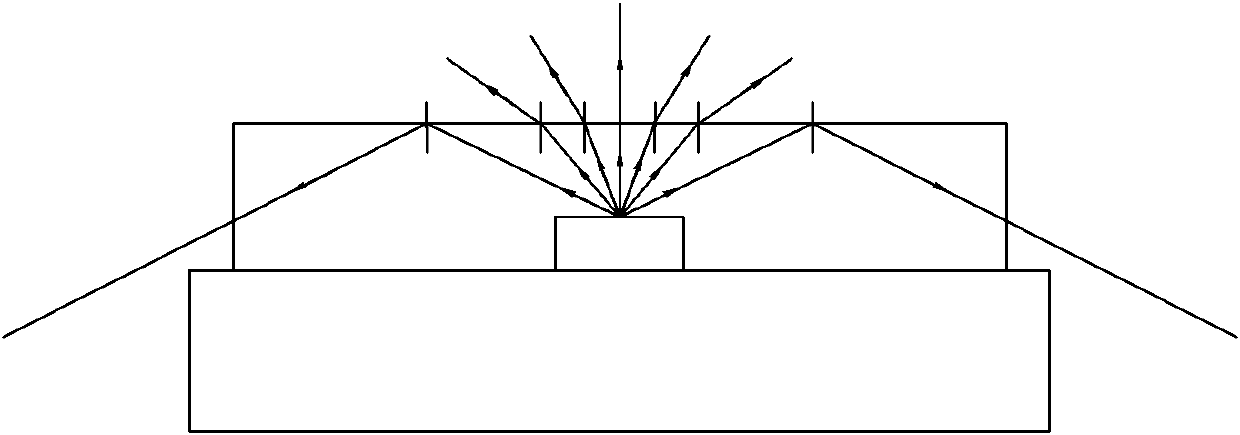
[0038] like Figure 6 ~ Figure 8As shown, the LED integrated light source board of this embodiment is a flat LED integrated light source board without a lens that can simultaneously produce multiple units and can be directly connected to 220V AC mains, including a thermally conductive insulating substrate 1, six interconnected Independent and unrelated LED light source units 30, the LED light source unit 30 includes 24 LED modules 31 connected in series, and each LED module 31 is composed of four LED chips 3 connected in series. The LED module 31 can also be composed of a single LED chip 3 alone. The thermally conductive insulating substrate 1 is a metal aluminum substrate. Of course, other metal substrates such as copper substrates can also be used. The upper surface of the metal substrate is provided with a thermally conductive insulating layer. 10. The surface of the thermally conductive insulating substrate 1 is laid with a circuit connection 21 and a heat dissipation foil...

Embodiment 2

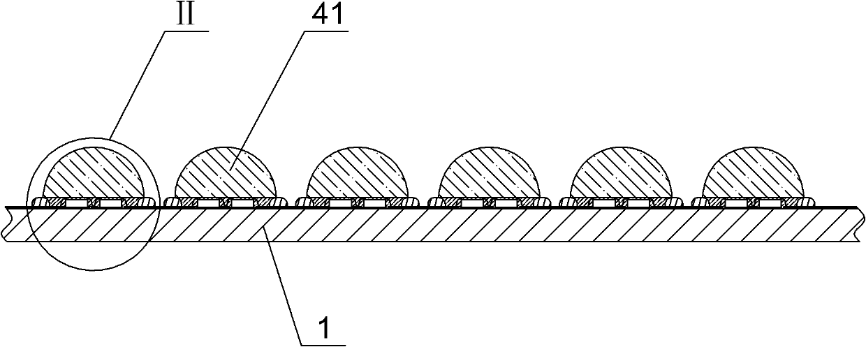
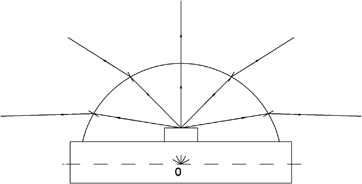
[0044] like Figure 9 , Figure 10 As shown, the difference between the LED integrated light source board of this embodiment and Embodiment 1 is that: in this embodiment, the thermally conductive and insulating substrate 1 is Al 2 o 3 Or AlN and other ceramic substrates, so the surface of the ceramic substrate does not need to be provided with a thermally conductive insulating layer; each of the LED modules 31 is covered with a spherical lens 41 in the light emitting direction, and the spherical lens 41 is cured by dispensing. Formed, the focal point of the spherical lens 41 is located in the same plane as the light emitting surface of the LED module 31, as image 3 As shown, at this time, the light emitted by the LED chip can be effectively emitted, and there will be no total reflection phenomenon. Under the same conditions, the light output rate can be increased by 5-20% compared with Embodiment 1. It is a light distribution design of a large-angle lens. When the luminous...


PUM


Abstract

The invention discloses an LED integrated light source board with low cost, simple structure and process, high production efficiency and high color temperature precision and a manufacturing method thereof. The light source board comprises a heat-conducting insulation substrate (1) and an LED light source unit (30), wherein, the LED light source unit (30) comprises a plurality of LED modules (31) formed by integrating a plurality of LED chips (3) or composed of the separate LED chip (3); a circuit connecting wire (21) and a radiating foil (22) which are composed of metal layers are laid on the surface of the heat-conducting insulation substrate (1); the LED modules (31) are electrically connected with the circuit connecting wire (21); the LED chips (3) are connected with a radiating foil (22) for conducting heat; and a white colloid coffer (4) the height of which is 0.3-1.5mm is coated around the LED modules (31), and silica gel or resin (6) is filled in the colloid coffer (4) to cover the LED chips (3). The manufacturing method comprises the following steps: die-bonding, forming the colloid coffer, filling the silica gel or the resin (6), and curing. The invention can be applied to the LED integrated light source field.

Description

technical field [0001] The invention relates to an LED integrated light source board; in addition, the invention also relates to a manufacturing method of the LED integrated light source board. Background technique [0002] As a new type of lighting source, LED is being more and more widely used in various occasions due to its outstanding advantages such as energy saving, environmental protection, high luminous efficiency, and long life. The application of high-power LED light sources in lamps can now be used as large lamps such as street lamps and wall washers. In high-power LED light sources, LED chips and lenses are generally packaged into in-line lamp beads or SMD packages. A light source board formed on the substrate and the copper substrate is called the second light source package, and is used for heat dissipation through the heat-conducting insulating substrate and as a substrate for circuit connection. Because it must be packaged by the secondary light source, the...

Claims


Application Information

Patent Timeline
Patent Type & Authority Applications(China)
IPC IPC(8): F21V19/00F21V29/00F21V5/04F21V29/74F21V29/85
Inventor 吴俊纬
Owner NANKER GUANGZHOU SEMICON MFG
Why Eureka
Try Eureka