Ion injection and plasma deposition equipment and method for processing films by using plasmas
A plasma and ion implantation technology, applied in the field of plasma treatment, can solve the problems of continuous ion implantation of workpieces to be processed, and achieve the effects of uniform and dense texture, reduction of production cost and improvement of production efficiency
- Summary
- Abstract
- Description
- Claims
- Application Information
AI Technical Summary
Problems solved by technology
Method used
Image
Examples
Embodiment 1
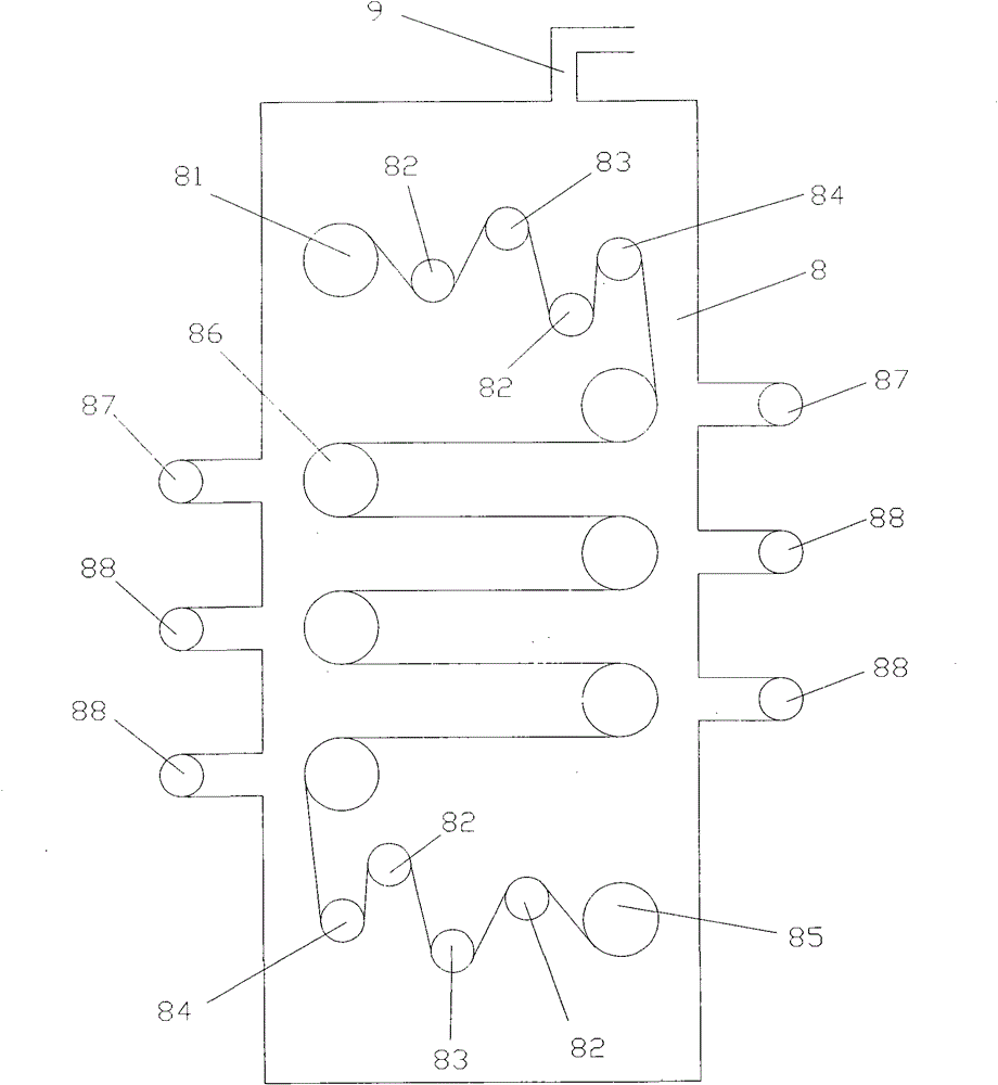
[0039] figure 2 The vacuum chamber part 8 of an ion implantation and plasma deposition thin film equipment provided by the present invention is provided with an unwinding roller 81, a transition wheel 82, a tension adjustment roller 83, a traction wheel 84, and a winding roller 85 , a cooling roller 86 , an opening 87 for ion implantation, an opening 88 for plasma deposition, and a vacuum port 9 .
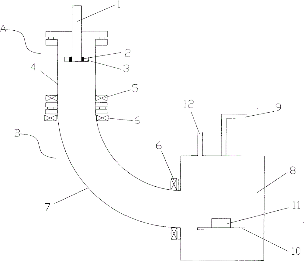
[0040] The opening for ion implantation and the opening for plasma deposition are respectively connected with a magnetic filter vacuum arc ion source (such as figure 1 Parts A and B in ) are connected, and there is also a voltage (not shown) between the openings 87 and 88 and B to accelerate the ion beam emitted by the ion source. The opening is rectangular, wherein the dimension of the side perpendicular to the axial direction of the cooling roller is 50 mm, and the dimension of the side in the other direction is 265 mm. The diameter of the cooling roll shaft is 70 mm, the dist...
Embodiment 2
[0042] Embodiment 2, deposit the copper film of 25 nanometers on each side of polyimide (PI) thin film (implantation copper+deposition copper)
[0043] Experimental process: (1) Place a roll of polyimide (PI) film (thickness 0.025 mm, width 270 mm) on the unwinding roller, pass one end of the PI film through the tension adjustment mechanism in turn, all cooling rollers, tension The adjustment mechanism is finally fixed on the winding device. Put cooling water at 0-10°C into the cooling roller, and vacuumize to make the vacuum degree 5×10 -4 Pa. Turn on the ion source and turn on the accelerating voltage. Run the PI film at 2 m / min.
[0044] (2) All copper ion sources are used. The ion implantation voltage is 5KV, and the implantation dose is 3×10 14 atoms / cm2; the plasma deposition voltage is 0.2KV, and the ion beam current is 40 mA. The thickness of the copper film on the obtained film is about 25 nanometers, and the texture of the metal layer is uniform and dense.
Embodiment 3
[0045] Embodiment 3, deposit the copper film of 200 nanometers on each side of polyimide (PI) thin film (implantation copper+deposition copper)
[0046] (1) Except that the running speed of the PI film is 0.3 m / min, all other operations are the same as step (1) in Example 2.
[0047] (2) All copper ion sources are used. The ion implantation voltage is 6KV, and the implantation dose is 1×10 16 atoms / cm 2 ; The plasma deposition voltage is 0.3KV, and the ion beam current is 70 mA. The thickness of the copper film (injected copper+deposited copper) on the obtained film is about 200 nanometers, and the texture of the metal layer is uniform and dense.
PUM
| Property | Measurement | Unit |
|---|---|---|
| diameter | aaaaa | aaaaa |
| thickness | aaaaa | aaaaa |
| thickness | aaaaa | aaaaa |
Abstract
Description
Claims
Application Information

