Unlock instant, AI-driven research and patent intelligence for your innovation.

TFT (Thin Film Transistor)-LCD (liquid Crystal Display) array substrate and manufacturing method thereof

A technology of an array substrate and a manufacturing method, which is applied in the field of TFT-LCD array substrates and its manufacture, can solve problems such as short circuits between gate lines and data lines, and achieve the effects of wide application prospects, reduced short circuits, and simple structure

Active Publication Date: 2013-02-13
K TRONICS (SUZHOU) TECH CO LTD +1
View PDF5 Cites 0 Cited by
  • Summary
  • Abstract
  • Description
  • Claims
  • Application Information

AI Technical Summary

Problems solved by technology

[0004] The purpose of the present invention is to provide a TFT-LCD array substrate and its manufacturing method, which can effectively overcome the defects of short-circuiting between gate lines and data lines caused by particles in the manufacture of existing TFT-LCD array substrates

Method used


Image

  • TFT (Thin Film Transistor)-LCD (liquid Crystal Display) array substrate and manufacturing method thereof
  • TFT (Thin Film Transistor)-LCD (liquid Crystal Display) array substrate and manufacturing method thereof
  • TFT (Thin Film Transistor)-LCD (liquid Crystal Display) array substrate and manufacturing method thereof

Examples


Embodiment Construction

[0047] The technical solutions of the present invention will be further described in detail below through the accompanying drawings and embodiments.

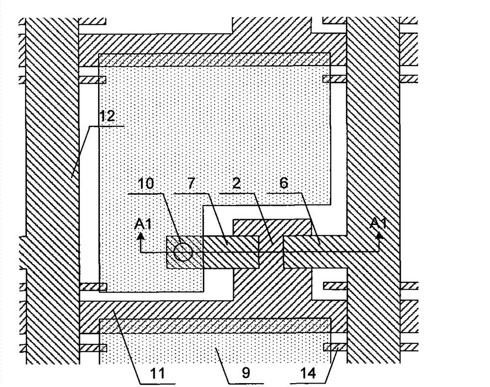
[0048] figure 1 It is a plan view of the first embodiment of the TFT-LCD array substrate of the present invention, which reflects the structure of a pixel unit, figure 2 for figure 1 Sectional view from the A1-A1 direction. Such as figure 1 with figure 2 As shown, the TFT-LCD array substrate of this embodiment is a structure formed by using four patterning processes. The main structure includes gate lines 11, data lines 12, pixel electrodes 9 and thin film transistors formed on the substrate 1, which are perpendicular to each other. The gate line 11 and the data line 12 define the pixel area, the thin film transistor and the pixel electrode 9 are formed in the pixel area, the gate line 11 is used to provide the turn-on signal to the thin film transistor, the data line 12 is used to provide the data signal to the pixel electrode 9....


PUM

PropertyMeasurementUnit
widthaaaaaaaaaa

Abstract

The invention relates to a TFT (Thin Film Transistor)-LCD (liquid Crystal Display) array substrate and a manufacturing method thereof. The array substrate comprises grid lines, data lines, a pixel electrode and a TFT which are formed on a substrate, wherein the side faces of the grid lines are provided with isolation dams used for avoiding the short circuits of the grid lines and the data lines; the isolation dams are strip-shaped bodies which are arranged at one side or two sides of the grid lines and overlapped with the data lines; and the strip-shaped bodies are arranged on the same layer as the grid lines and formed in the same structure composition process. In the invention, a plurality of edge structures are formed near crossing regions of the grid lines and the data lines, on one hand, the density of adhesion particles at each edge is reduced through increasing the edge structures, and one the other hand, the particles are absorbed to adhere by utilizing the edges of the isolation dams to finally reduce the probability of dropping the particles on the edges of the grid lines and furthest reduce the short circuits of the grid lines and the data lines. Compared with the measure of solving the short circuit problem of the grid lines and the data lines resulting from the particles in the prior art, the technical scheme has the advantages of simple structure, convenient construction and obvious effect.

Description

Technical field [0001] The invention relates to a thin film transistor liquid crystal display and a manufacturing method thereof, in particular to a TFT-LCD array substrate and a manufacturing method thereof. Background technique [0002] Thin Film Transistor Liquid Crystal Display (TFT-LCD) has the characteristics of small size, low power consumption, and no radiation, and it occupies a dominant position in the current flat panel display market. For TFT-LCD, the structure of the array substrate largely determines the yield and price. The manufacture of TFT-LCD array substrates is completed by multiple sets of deposition and patterning processes to form different film patterns. After each layer of film is deposited, through photoresist coating, masking, exposure, etching and photoresist stripping processes A layer of thin film pattern is formed, and finally the TFT-LCD array substrate is formed by the multilayer thin film pattern. [0003] At present, the particle problem in the ...

Claims


Application Information

Patent Timeline
Patent Type & Authority Patents(China)
IPC IPC(8): G02F1/1362G02F1/1368H01L21/82
Inventor 彭志龙董云刘玉清
Owner K TRONICS (SUZHOU) TECH CO LTD