
Flow soldering apparatus and flow soldering method

A technology of flow soldering and flux, applied in tin feeding device, welding equipment, assembling printed circuit with electrical components, etc., can solve problems such as welding defects

Inactive Publication Date: 2011-01-26
PANASONIC CORP
View PDF0 Cites 2 Cited by
  • Summary
  • Abstract
  • Description
  • Claims
  • Application Information

AI Technical Summary

Problems solved by technology

Therefore, with the flow soldering apparatus described above, there is a risk that soldering defects may occur

Method used


Image

  • Flow soldering apparatus and flow soldering method
  • Flow soldering apparatus and flow soldering method
  • Flow soldering apparatus and flow soldering method

Examples


Embodiment Construction

[0044] Description of the embodiment

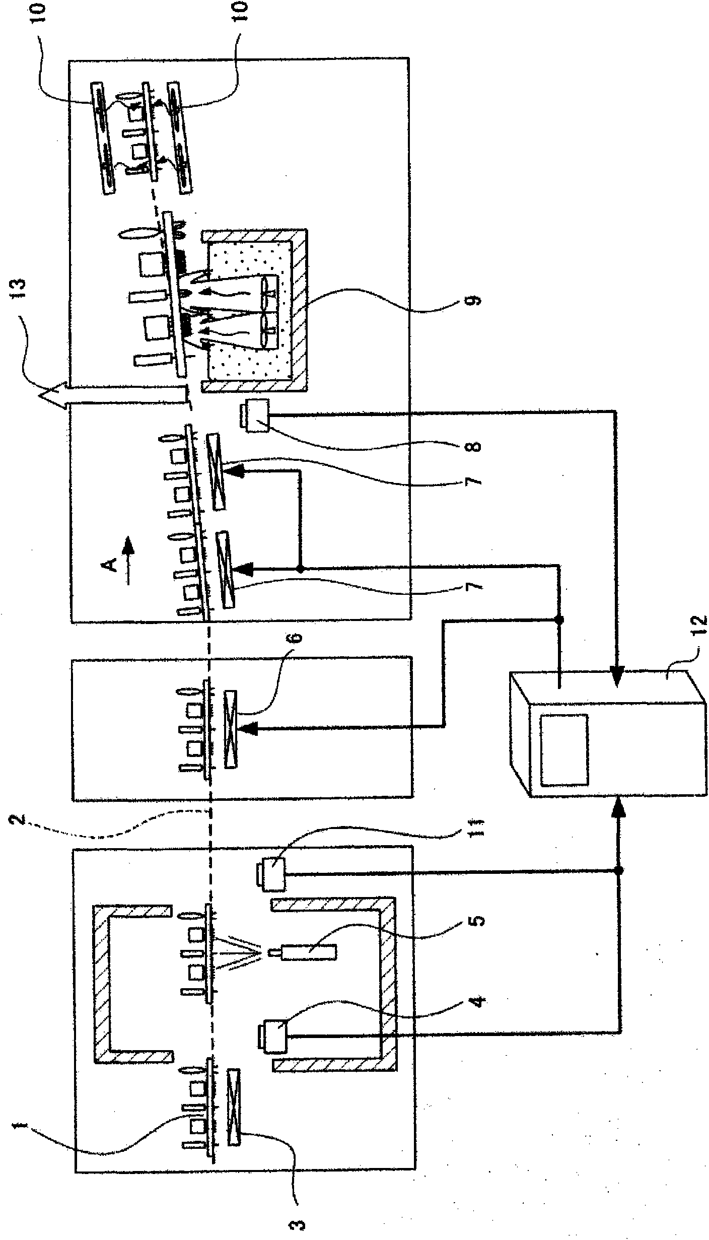
[0045] figure 1 is a diagram showing one example of the composition of the flow soldering apparatus according to the embodiment of the present invention. A moisture sensor is incorporated into the flow soldering line and the preheat profile is controlled by feedback control based on the signal provided by the moisture sensor. First, an overview of the composition of the present flow soldering apparatus is described.

[0046] Such as figure 1 As shown, the electronic circuit substrate 1 formed with a plurality of through holes is transferred into the flow soldering device. Electronic components were previously mounted on the component surface of the electronic circuit substrate 1 introduced into the device. Leads of electronic components mounted on this substrate are inserted into through holes of the electronic circuit substrate 1 and protrude from the soldering surface.

[0047] The conveyor 2 is arranged in the flow soldering devic...


PUM

PropertyMeasurementUnit
heightaaaaaaaaaa
diameteraaaaaaaaaa

Abstract

The present invention provides a flow soldering apparatus that can suppress the occurrence of soldering defects, even if VOC-free flux or low-VOC flux is applied to an electronic circuit substrate. In other words, the flow soldering apparatus according to the present invention includes: a water content sensor for measuring a residual water content of a surface of a substrate; and a monitoring device for judging whether soldering quality is satisfactory or not by using a residual water content value of the surface of the substrate acquired from the residual water content measured by the water content sensor, on the basis of a correlation between a residual water content value of a surface of a sample substrate and a residual water content value of through holes of the sample substrate, as acquired previously by using a plurality of substrate samples.

Description

technical field [0001] The invention relates to a flow soldering device and a flow soldering method suitable for VOC-free flux or low-VOC flux. VOC is the abbreviation of Volatile Organic Compounds. Background technique [0002] Flow soldering is a technique used to solder electronic components to electronic circuit substrates. An overview of this technique is described below. First, electronic components are mounted on one main surface of an electronic circuit substrate. The leads of the mounted electronic components are inserted into the through holes in the electronic circuit substrate, and protrude from the other main surface of the electronic circuit substrate. Molten solder contacts the lead protrusions on the surface, thereby soldering the electronic component to the electronic circuit substrate. Hereinafter, one main surface on which the electronic component is mounted is referred to as the component surface, and the other main surface on which molten solder esta...

Claims


Application Information

Patent Timeline
Patent Type & Authority Applications(China)
IPC IPC(8): H05K3/34
CPCH05K2203/163H05K3/3489H05K3/3447H05K3/3468H05K2201/10151B23K3/0653H05K2203/111H05K2203/0126
Inventor 中谷公明末次宪一郎岸新
Owner PANASONIC CORP
Learn More