Method for growing GeSn alloy on Si substrate by molecular beam epitaxy

A technology of molecular beam epitaxy and epitaxial growth, which is applied in the field of semiconductor thin film material preparation, can solve the problems of insufficient material quality, failure to reach device-level materials, and poor thermal stability of materials, etc.

Inactive Publication Date: 2011-02-02
INST OF SEMICONDUCTORS - CHINESE ACAD OF SCI
View PDF1 Cites 24 Cited by
  • Summary
  • Abstract
  • Description
  • Claims
  • Application Information

AI Technical Summary

Problems solved by technology

Although these two methods have each achieved some results, they are still relatively preliminary.
Although the best GeSn material has been obtained by UHV-CVD growth, the quality of the material is not good enough, and it cannot reach the level of device-level materials, and the Sn source-SnD4 used is difficult to prepare; while the material grown by MBE The thermal stability is relatively poor, and Sn is easy to segregate; therefore, the growth of GeSn alloy materials needs breakthroughs in new technologies and methods

Method used


Image

  • Method for growing GeSn alloy on Si substrate by molecular beam epitaxy
  • Method for growing GeSn alloy on Si substrate by molecular beam epitaxy
  • Method for growing GeSn alloy on Si substrate by molecular beam epitaxy

Examples


no. 1 example

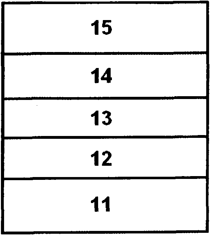
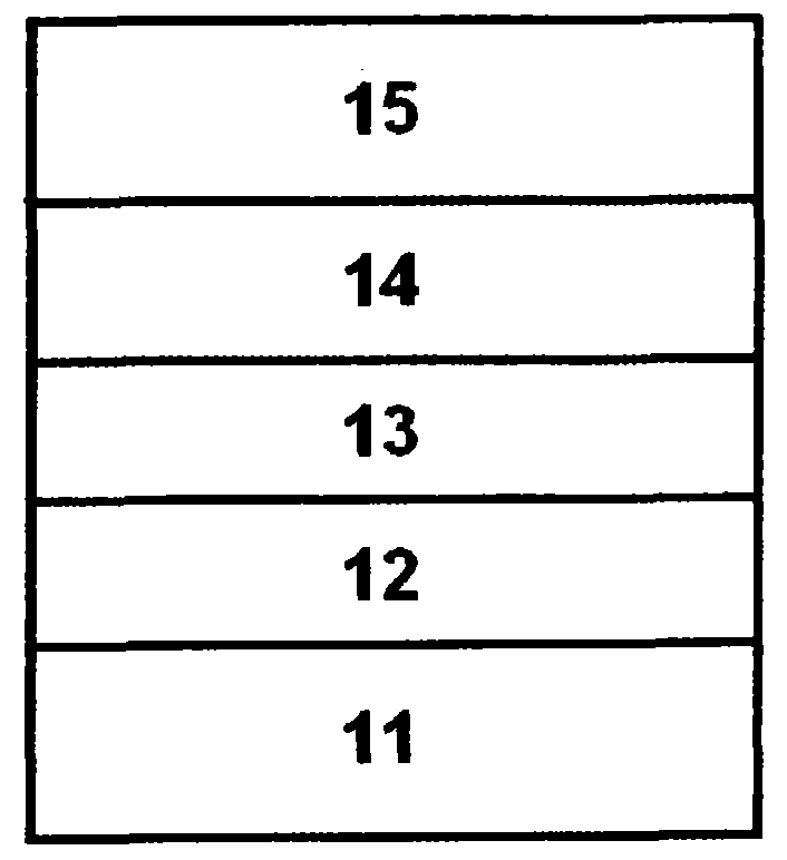
[0028] Please see attached figure 1 , which is the first embodiment of the present invention, which is a method for growing Si-based GeSn alloys by a low-temperature two-step method. It includes the following steps:

[0029] Step 1: growing a first Ge material layer 12 on the Si substrate 11, and the growth temperature of the first Ge material layer 12 is less than 400°C;

[0030] Step 2: growing a second Ge material layer 13 on the first Ge material layer 12, and the growth temperature of the second Ge material layer 13 is greater than 400°C;

[0031] The first and second Ge material layers are grown using solid Ge as the source material and grown by molecular beam epitaxy; the first and second Ge material layers are GeH 4 and Ge 2 H 6 The compound of Ge and H is used as the source material, which is grown by chemical vapor deposition method;

[0032] Step 3: growing a first GeSn alloy layer 14 on the second Ge material layer 13, the first GeSn alloy layer 14 is grown by...

no. 2 example

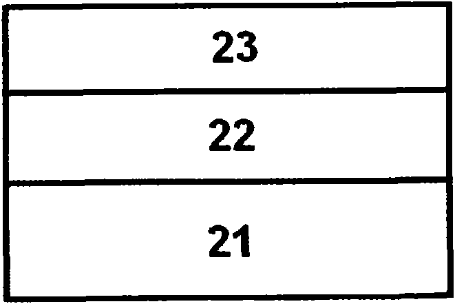
[0044] Attached below figure 2 Another implementation method of the present invention is illustrated.

[0045] see again figure 2 Shown, a kind of method of molecular beam epitaxial growth GeSn alloy of the present invention on Si substrate comprises the steps:

[0046] Step 1: On the Si substrate 21, using solid Ge material and solid Sn material as Ge source and Sn source respectively, using molecular beam epitaxy system to deposit a first GeSn alloy layer 22 with a thickness of 25nm, the growth temperature is 100°C ;

[0047] Step 2: on the first GeSn alloy layer 22, adopt solid Ge material and solid Sn material as Ge source and Sn source respectively, utilize the molecular beam epitaxy system to deposit the second GeSn alloy layer 23 with a thickness of 300nm, the growth temperature is 180°C.


PUM


Abstract

The invention provides a method for growing GeSn alloy on a silicon (Si) substrate by molecular beam epitaxy. The method comprises the following steps of: 1, growing a first Ge material layer on the Si substrate; 2, growing a second Ge material layer on the first Ge material layer; 3, growing a first GeSn alloy layer on the second Ge material layer; and 4, growing a second GeSn alloy layer on the first GeSn alloy layer to finish the growth of the material.

Description

technical field [0001] The invention relates to the preparation technology of semiconductor thin film materials, and more particularly, the invention provides a method for epitaxial growth of GeSn alloy on Si substrate. Background technique [0002] Si is the foundation of modern microelectronics technology. Due to the advantages of mature technology, low price and abundant source materials, Si microelectronics technology has an irreplaceable position in the modern electronic information society. The development of Si microelectronics technology has penetrated into all aspects of the national economy, national security and people's daily life. For example, more than 90% of the electronic devices and circuits in the world are based on Si. However, the use of electrons as the information carrier in microelectronics technology has its own limitations, and it is difficult to meet the urgent needs of the future information society for information transmission capacity, processin...

Claims


Application Information

Patent Timeline
Patent Type & Authority Applications(China)
IPC IPC(8): H01L21/20C30B23/02C30B25/02
Inventor 苏少坚汪巍成步文王启明张广泽胡炜玄白安琪薛春来左玉华
Owner INST OF SEMICONDUCTORS - CHINESE ACAD OF SCI
Why Eureka
Try Eureka