

Measuring method and device for characterizing a semiconductor component
A measurement method and semiconductor technology, which is applied in the direction of single semiconductor device testing, measuring equipment, measuring electricity, etc., to achieve the effects of simplified analysis and processing and low equipment cost
- Summary
- Abstract
- Description
- Claims
- Application Information
AI Technical Summary
Problems solved by technology
Method used
Image


Examples
Embodiment Construction
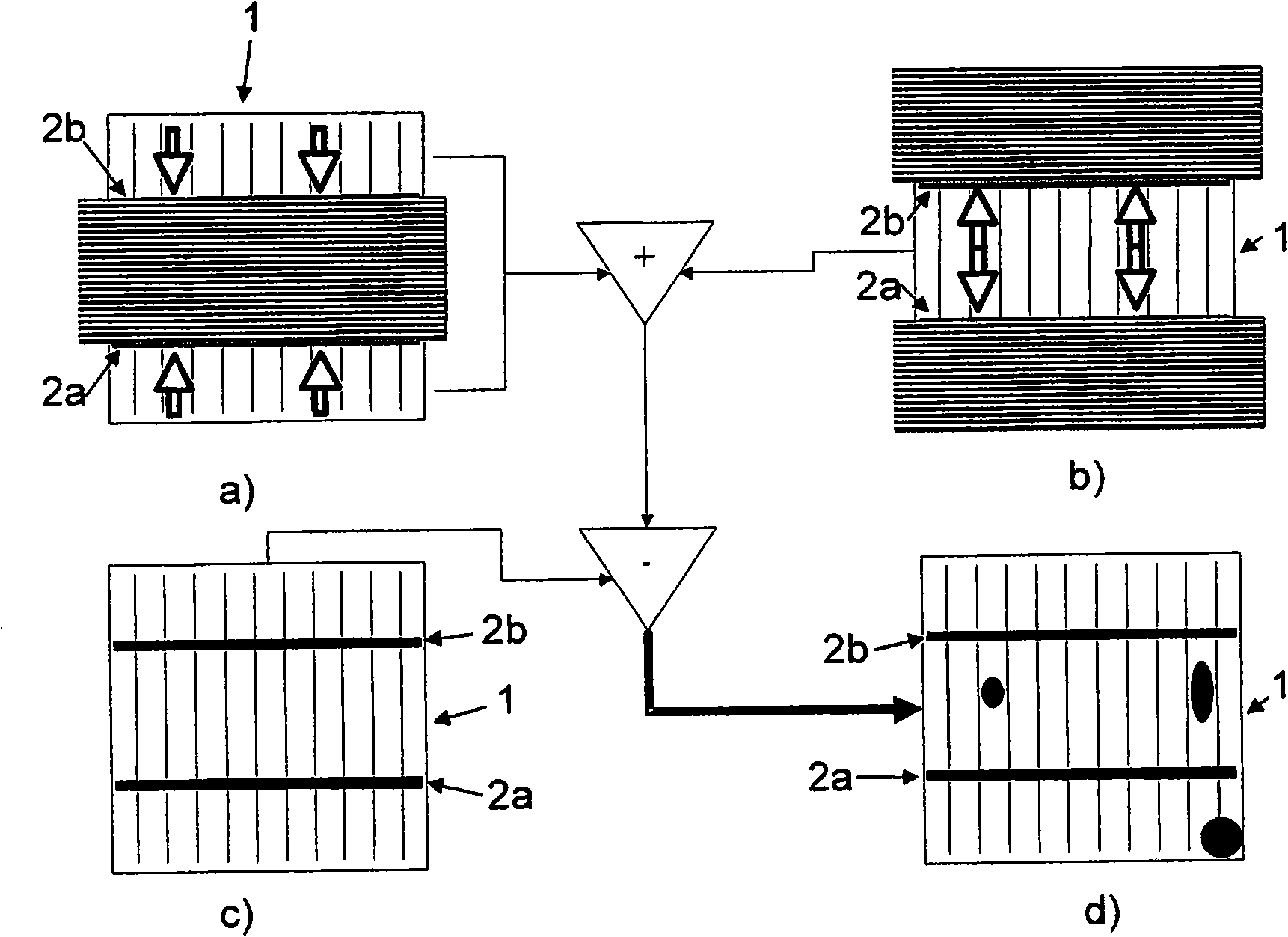
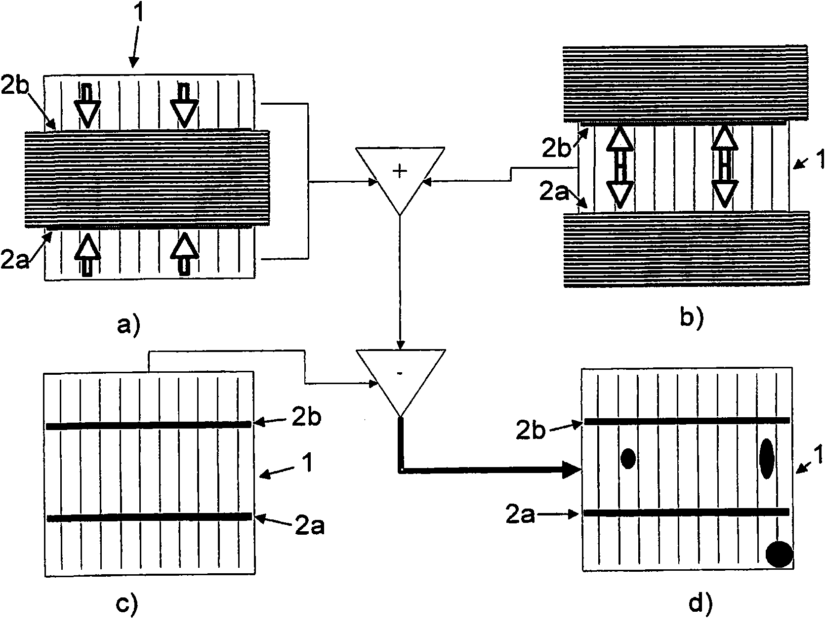
[0094] figure 1 The application of an exemplary embodiment of the measuring method according to the invention for measuring a semiconductor component 1 designed as a solar cell with two metallization lines 2 a and 2 b running parallel to one another is shown, which metallization The lines are the bus bars of the metallization structure.
[0095] For the measurement, a conventional photoluminescence measuring device is used which is extended with a correction unit with two optical filters.
[0096] During the measurement, the battery is not electrically connected. A total of three measurements were carried out, wherein in each measurement the cameras of the measuring device were photographed with a measurement time of one second in each case. The three measurements differ only in the shielding conditions for the excitation beam. The measuring surfaces are respectively figure 1 Front side of the solar cell shown in a,b,c,d.
[0097] In the first measurement ( figure 1 a) I...
PUM
 Abstract
Description
Claims
Application Information