
Simultaneous ion milling and sputter deposition

a technology of sputter deposition and ion milling, which is applied in the direction of electrolysis components, vacuum evaporation coatings, coatings, etc., can solve the problems of copper not sticking well to oxide, difficult uniform sidewall and bottom coverage, and complicated situation, etc., to achieve uniform time-integrated beam intensity

Inactive Publication Date: 2007-03-08
APPLIED MATERIALS INC
View PDF19 Cites 25 Cited by
  • Summary
  • Abstract
  • Description
  • Claims
  • Application Information

AI Technical Summary

Benefits of technology

[0015] The width of the aperture may be varied along its length to control the local beam intensity and need not be continuous. For example, the width in the central portion of the straight sections may be decreased over the width at the outer portions to compensate for geometrical effects and thereby make the time-integrated beam intensity more uniform across the rotating wafer.

Problems solved by technology

Sputtering is fundamentally a ballistic process which is ill suited to penetrating deeply into such holes.
The situation is somewhat more complicated if the conductive feature is a semiconducting silicon portion formed in a silicon substrate, but the metallization problems are much the same.
Also, copper does not stick well to oxide.
Furthermore, the unbalanced magnetron produces magnetic components which project from the target toward the wafer, thus expanding the plasma and guiding the metal ions toward the wafer.
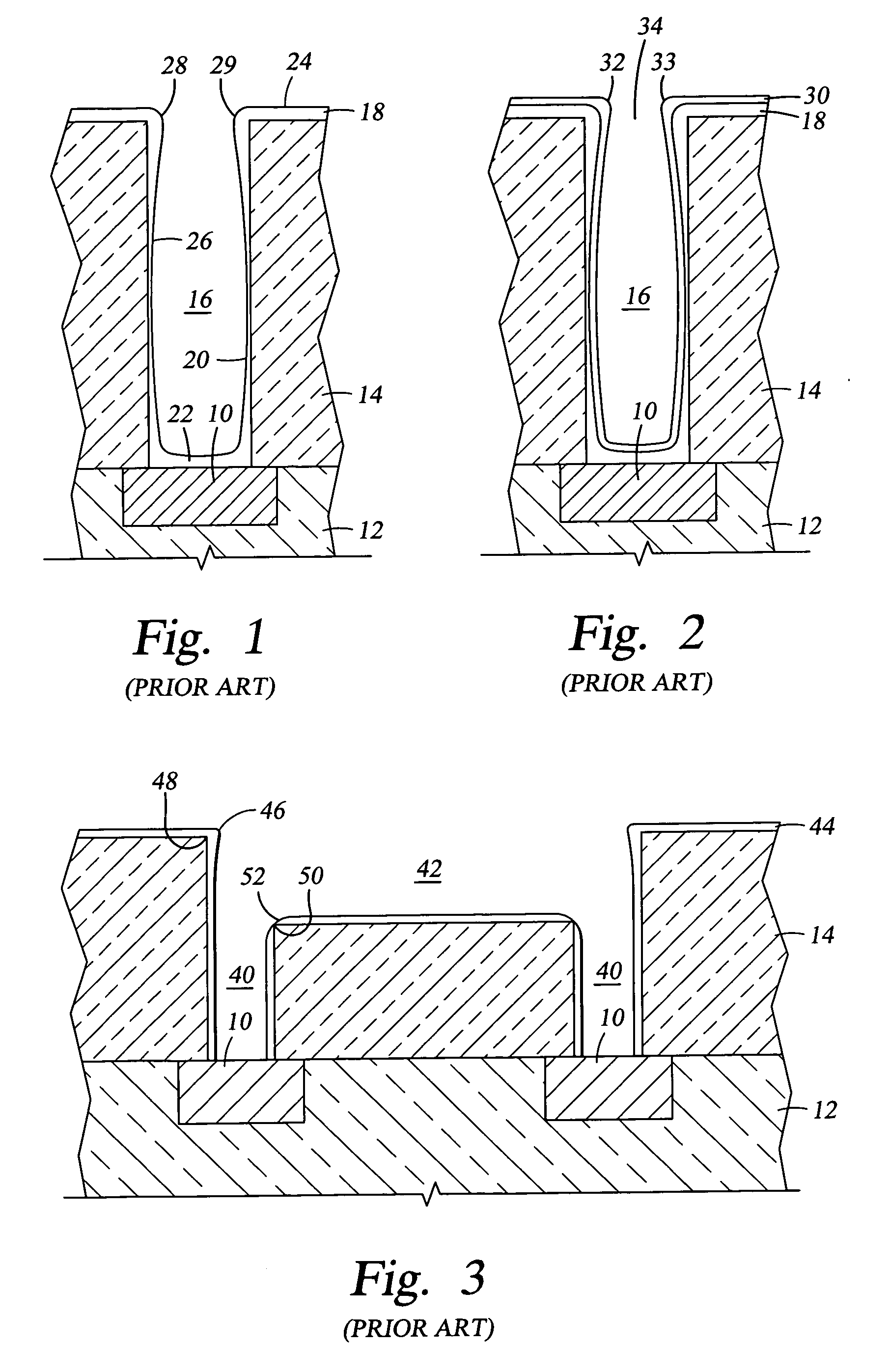
Such overhangs 28 significantly increase the effective aspect ratio of the hole during the final stages of the barrier deposition, thus making the uniform sidewall and bottom coverage even more difficult.
However, sputtering copper into the via hole 16 partially closed by the barrier overhangs 28 is difficult because of the high effective aspect ratio.
Even if the via hole 16 remains unbridged at the beginning of the electrochemical plating (ECP) copper fill, the constricted throat 34 presents significant problems to completing the ECP fill.
However, shaped targets are significantly more expensive than planar targets.
However, this technique has its limitations.
That is, the barrier may be removed at the corner, whether in barrier or metallization sputter deposition, a very unfavorable result.
Furthermore, excessively high biasing also tends to sputter etch rather than sputter deposit at the bottom of the hole, an effect that needs to be carefully considered.
One problem with previous approaches to ion milling has been the poor milling uniformity across the wafer.

Method used


Image

  • Simultaneous ion milling and sputter deposition
  • Simultaneous ion milling and sputter deposition
  • Simultaneous ion milling and sputter deposition

Examples


Embodiment Construction

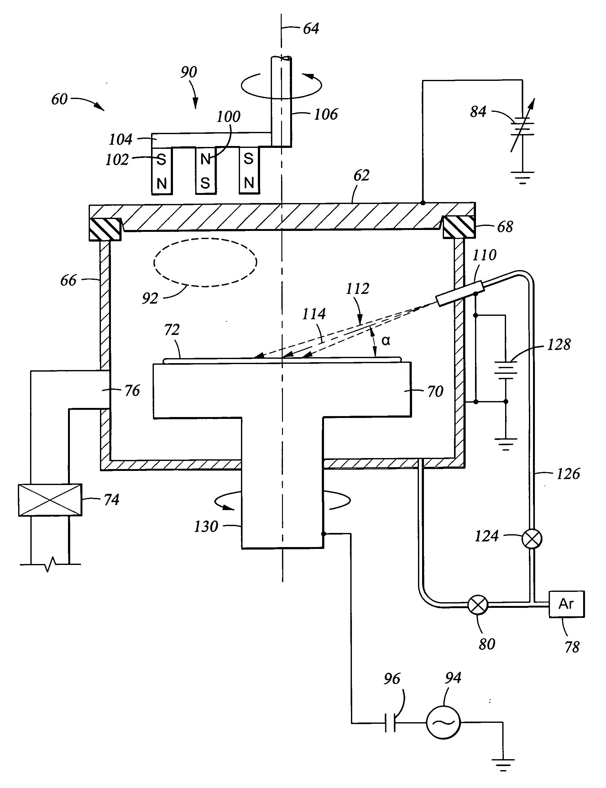
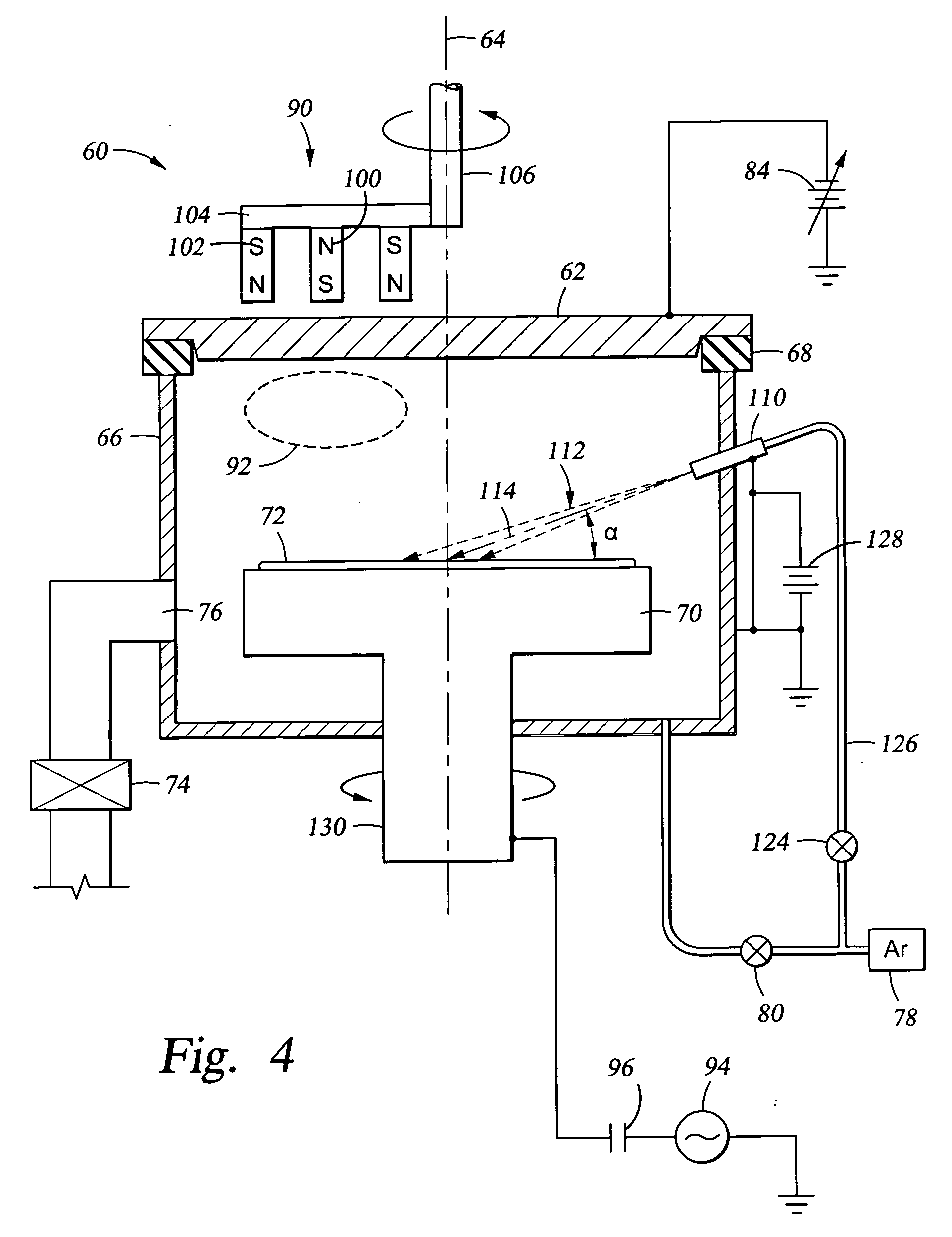
[0029] One aspect of the invention improves upon an an embodiment of Gopalraja but uses a single linear ion beam directed at the diameter of a rotating wafer. A sputtering reactor 60 schematically illustrated in FIG. 4 is based upon a self-ionized plasma (SIP) reactor available from Applied Materials and includes many standard components of the commercialized reactor which will be first described. The plasma sputter reactor 60 includes a planar target 62 arranged about a central axis 64 and supported on a grounded chamber body 66 through an annular isolator 68. At least the surface portion of the target 62 is composed of the material to be sputtered, but copper targets are typically fabricated of solid copper. A pedestal electrode 70 supports a wafer 72 to be sputter coated in opposition to the target 62 along the central axis 64 and includes unillustrated chilling fluid lines and thermal transfer gas cavities for controlling the wafer temperature. Unillustrated shields, at least on...


PUM

PropertyMeasurementUnit
inclined angleaaaaaaaaaa

Abstract

A magnetron sputter reactor including an ion beam source producing a linear beam that strikes the wafer center at an angle of less than 35°. The linear beam extends across the wafer perpendicular to the beam but has a much short dimension along the beam propagation axis while the wafer is being rotated. The ion source may be an anode layer source having a plasma loop between an inner magnetic pole and a surrounding outer magnetic pole with anode overlying the loop with a closed-loop aperture. The beams from the opposed sides of the loop are steered together by making the outer pole stronger than the inner pole. The aperture width may be varied to control the emission intensity.

Description

FIELD OF THE INVENTION [0001] The invention relates generally to sputtering of materials. In particular, the invention relates to the combination of sputtering and etching or milling performed in the same chamber. BACKGROUND ART [0002] Sputtering, alternatively called physical vapor deposition (PVD) in its most common implementation, is widely used to deposit layers of metals and related materials in the fabrication of semiconductor integrated circuits. Typically, a target of the material to be sputtered is placed in opposition to a generally circular wafer to be sputter coated with a material at least partially originating from the target. Electrical means discharge an argon working gas into a plasma, and the resulting positively charged argon ions are attracted to the negatively biased target with enough energy to dislodge (sputter) atom-sized metal particles from the target. Some of these particles travel to the wafer and are deposited in a layer on the wafer surface. In reactive...

Claims


Application Information

Patent Timeline
Patent Type & Authority Applications(United States)
IPC IPC(8): C23C14/00
CPCC23C14/3442C23C14/345H01J37/3408H01J37/3056C23C14/35
Inventor TANG, XIANMINSUBRAMANI, ANANTHAGOPALRAJA, PRABURAMFU, JIANMINGYU, JICK
Owner APPLIED MATERIALS INC
Learn More