Semiconductor packaging structure and manufacture process thereof

A technology of manufacturing process and packaging structure, applied in semiconductor/solid-state device manufacturing, semiconductor devices, semiconductor/solid-state device components, etc., can solve problems such as substrate packaging colloid surface pollution, protective glue residue, etc.

Active Publication Date: 2011-02-16
ADVANCED SEMICON ENG INC
View PDF2 Cites 4 Cited by
  • Summary
  • Abstract
  • Description
  • Claims
  • Application Information

AI Technical Summary

Problems solved by technology

[0006] The purpose of the present invention is to provide a semiconductor packaging structure and its manufacturing process, which can avoid the problem of sur

Method used


Image

  • Semiconductor packaging structure and manufacture process thereof
  • Semiconductor packaging structure and manufacture process thereof
  • Semiconductor packaging structure and manufacture process thereof

Examples


Embodiment Construction

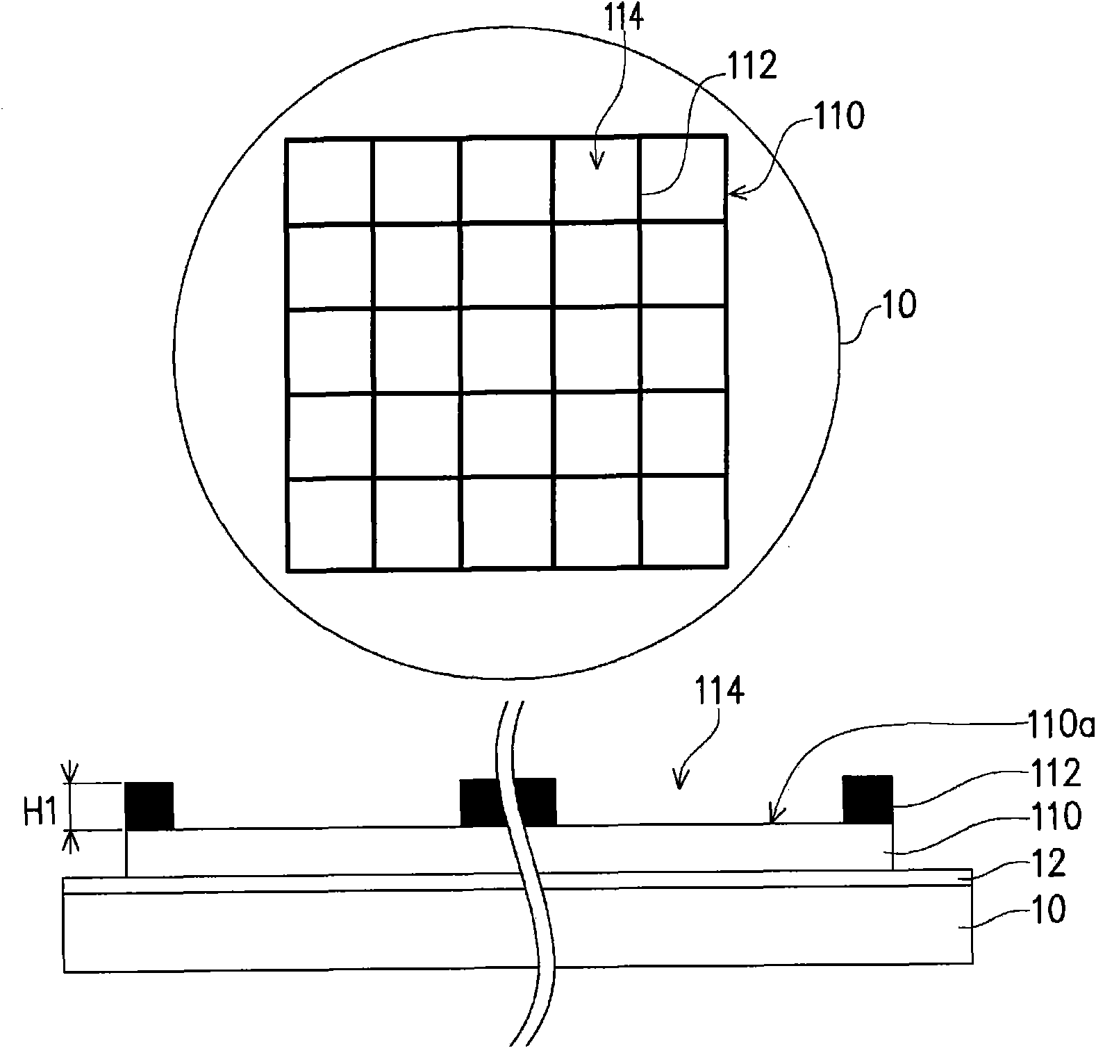
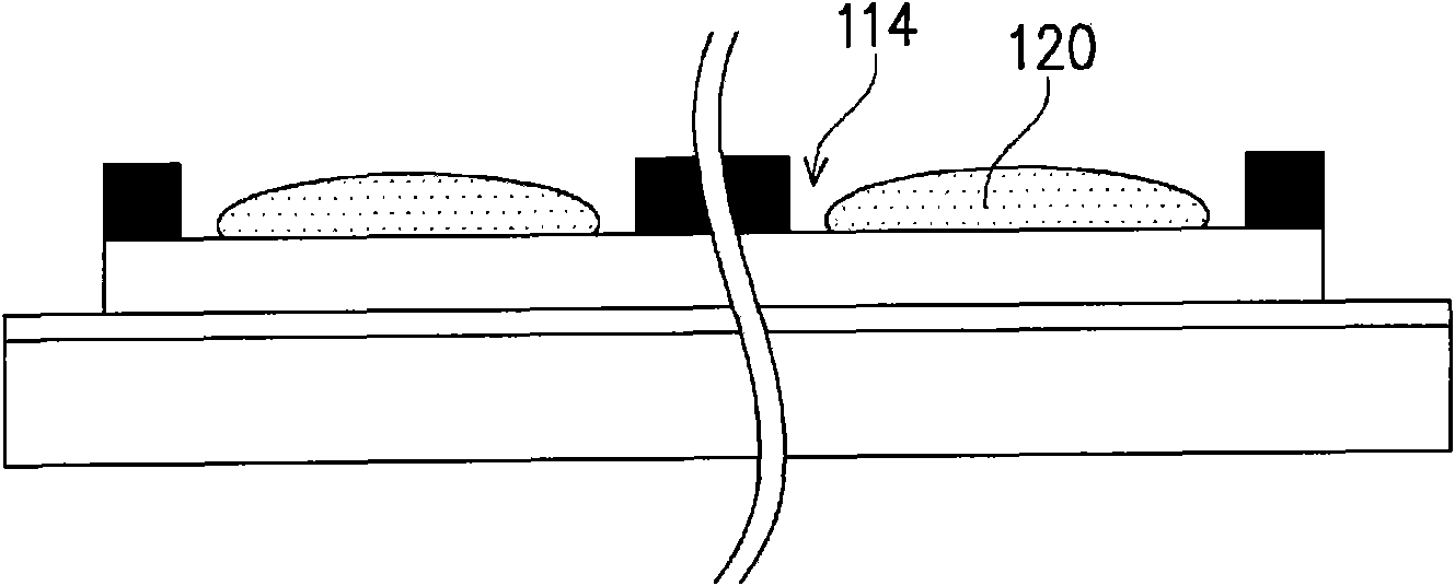
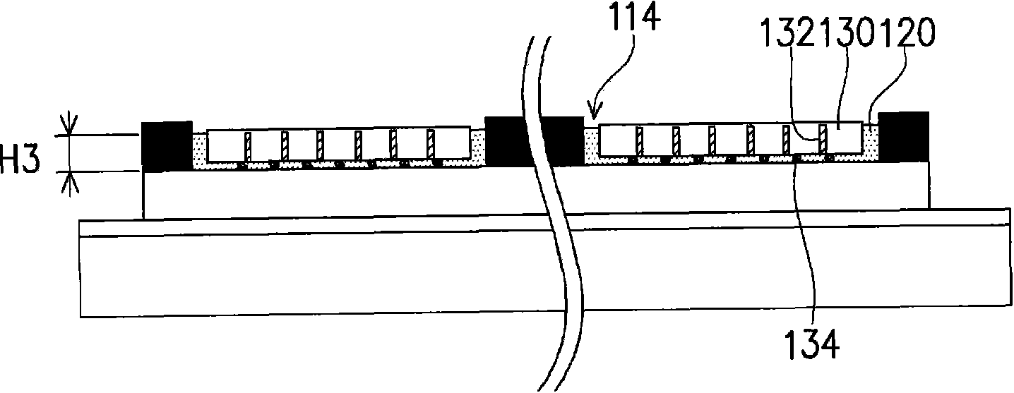
[0061] The present invention sets a grid wall with sufficient thickness on the packaging motherboard, wherein the grid wall can be integrated into the existing substrate manufacturing process, for example, the solder mask layer on the mounting surface of the packaging motherboard is thickened to form The grid wall, and the thickness of the grid wall is preferably controlled to be greater than the thickness of the thinned underlying chip. After the lower chip is bonded to the package motherboard and filled with primer, the package motherboard will be fully coated with a cladding layer to facilitate subsequent grinding steps. Since the thickness of the grid wall is greater than the thickness of the thinned lower chip, when the lower chip is ground to the end of the TSV, the cladding layer that was originally located above the grid wall and the lower chip is already in the grinding process. The middle layer is completely removed, so there will be no residual coating layer and its...


PUM


Abstract

The invention discloses a semiconductor packaging structure and a manufacture process thereof. The manufacture process of the semiconductor packaging structure comprises the steps of: configuring a packaging mother board on a support tool, wherein the packaging mother board is provided with a grid wall arranged vertically on the packaging mother board and the grid wall defines a plurality of concave parts on the packaging mother board; respectively jointing a plurality of first chips to the concave parts of the packing mother board, wherein each first chip is provided with silicon penetrating guide holes inside; forming first primer between each first chip and the corresponding packaging mother board; forming a cladding layer on the support tool; thinning the cladding layer and the grid wall from the upside of the support tool until the cladding layer above the grid wall and the first chip is completely removed; jointing a plurality of second chips to the first chips; forming second primer between each second chip and the corresponding first chip; separating the support tool from the packaging mother board, and cutting the packaging mother board to obtain a plurality of packaging units.

Description

technical field [0001] The invention relates to a semiconductor packaging technology, and in particular to a stacked semiconductor element packaging technology. Background technique [0002] In today's information society, the design of electronic products is moving toward light, thin, short, and small. Therefore, packaging technologies such as stacked semiconductor device packaging have been developed that are conducive to miniaturization. [0003] Stacked semiconductor element packaging is to package multiple semiconductor elements in the same package structure by vertical stacking, which can increase the packaging density to make the package miniaturized, and can shorten the signal transmission between semiconductor elements by using three-dimensional stacking The path length can increase the speed of signal transmission between semiconductor components, and semiconductor components with different functions can be combined in the same package. [0004] An existing stacke...

Claims


Application Information

Patent Timeline
IPC IPC(8): H01L21/50H01L23/29H01L23/13H01L21/58
CPCH01L2224/73204
Inventor 陈仁川张惠珊张文雄张唯农
Owner ADVANCED SEMICON ENG INC
Why Eureka
Try Eureka