Protecting component

A technology for protecting components and components, applied in electrical components, emergency protection devices, circuits, etc., can solve the problems of difficulty in cost reduction, unsatisfactory, and difficult to achieve compactness, and achieve the effect of easy assembly and manufacturing.

Active Publication Date: 2011-03-23
SCHOTT JAPAN CORP
View PDF10 Cites 5 Cited by
  • Summary
  • Abstract
  • Description
  • Claims
  • Application Information

AI Technical Summary

Problems solved by technology

Therefore, not only is it not ideal for applications to mobile information devices that require miniaturization and thinning, but there are also problems in assembly and manufacturing.
On the other hand, when forming a film resistor, it is difficult to obtain a desired resistance value on the characteristic surface while printing a ruthenium oxide-based paste and firing it at a temperature exceeding 800°C to obtain a uniform thick film resistor. , therefore, the trimming adjustment of thick film resistors becomes a laborious operation, and it is difficult to reduce the cost
In addition, the resistive film is not only small in size and can withstand less power, but also cannot be sintered from the resistive film to the organic substrate.
In addition, because it is formed on the back side where the lead wires for leading out are mounted, insulation treatment is required, and it is impossible to provide a protective element that satisfies miniaturization and thinning, and it is difficult to achieve compactness and lower backside as much as possible.

Method used


Image

  • Protecting component
  • Protecting component
  • Protecting component

Examples


Embodiment 1

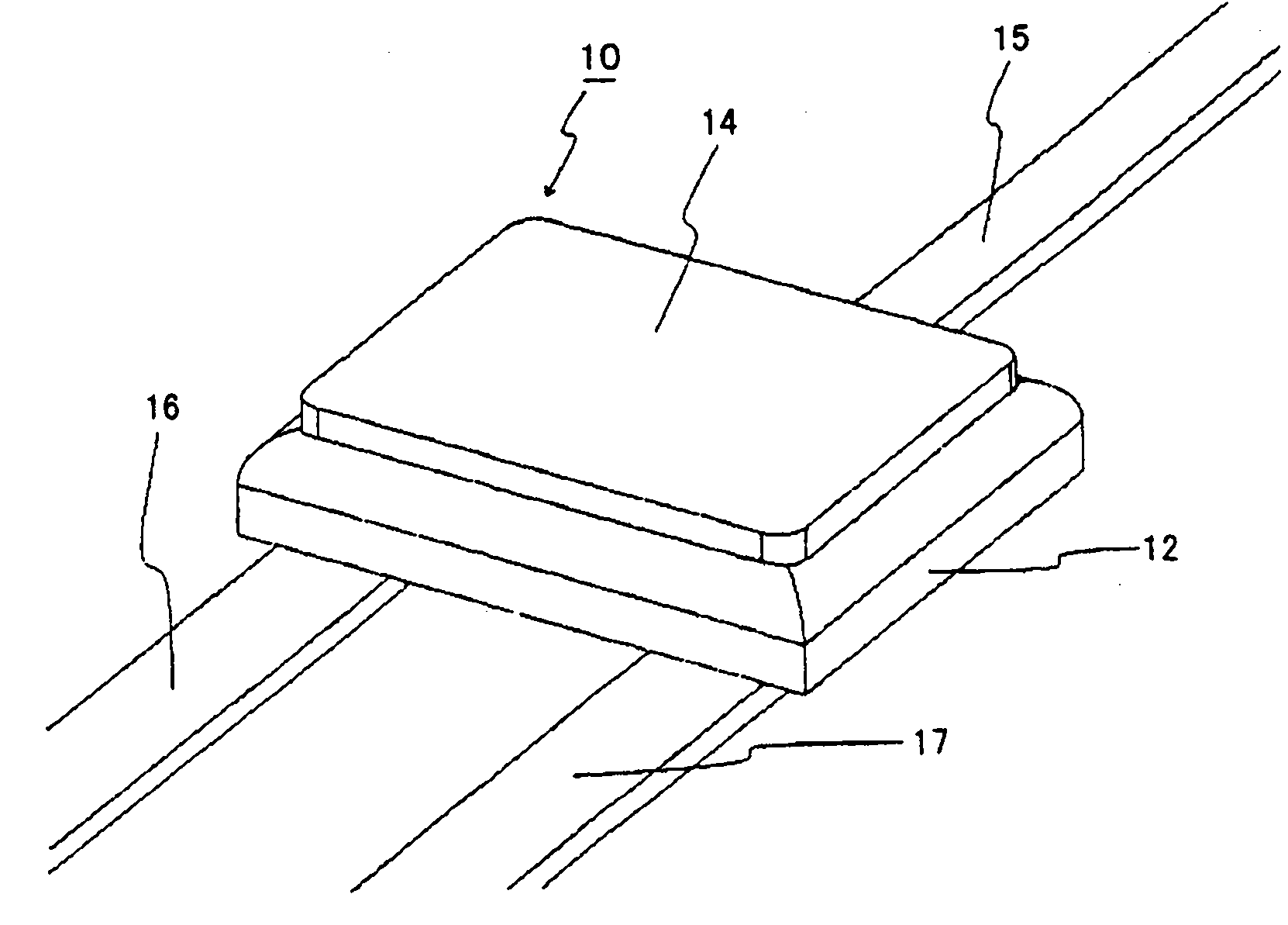
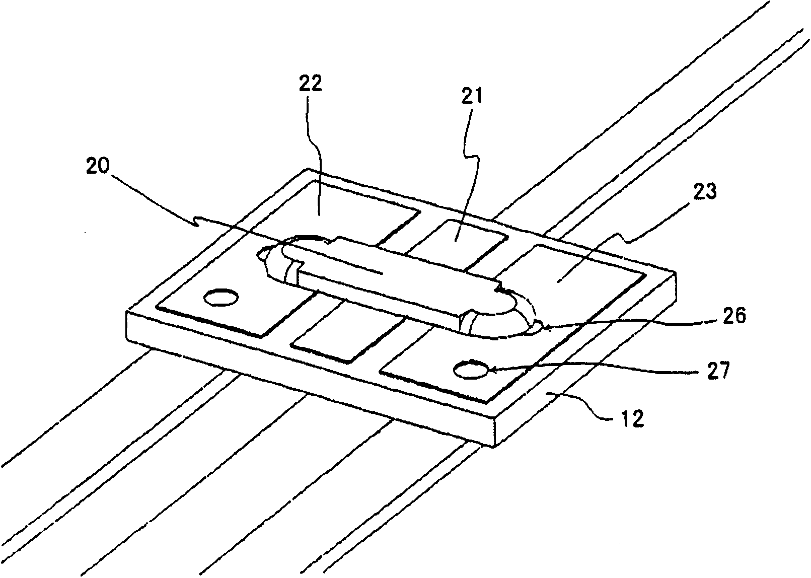
[0043] Hereinafter, a first embodiment of the present invention will be described in detail with reference to the drawings. The axial lead type protection element 10 of the present invention is as figure 1 As shown in a perspective view on its surface side, it includes: a ceramic chip body 12; A fuse element, a resistance heating element in the through hole, etc.; and lead-out leads 15-17, and these lead-out leads 15-17 are connected to the pattern electrodes on the back side. Here, patterned electrodes are formed on both surfaces of the ceramic chip body 12, a fusible alloy fuse element is installed on the surface side, lead wires for leading out are installed on the back side, and a resistance heating element is installed in the through hole of the chip body. . figure 2 It is a perspective view showing the state before the housing cover 14 of the package is mounted. On the pattern electrodes 21 to 23 provided on the ceramic chip body 12, a fusible alloy fuse element 20 wh...

Embodiment 2

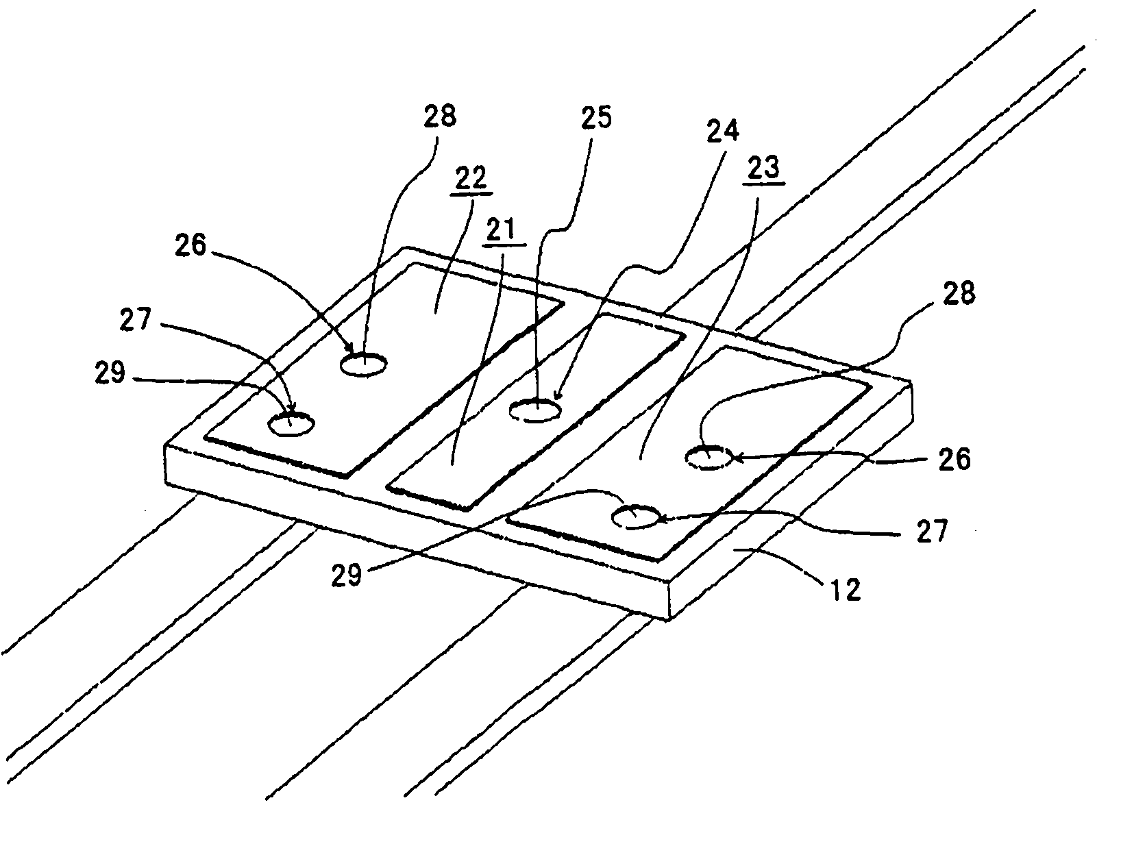
[0046] Other embodiments of the present invention are Figure 4 The chip-type protective element 30 shown in the perspective view of FIG. Figure 4 A perspective view showing the surface side with the protective cover removed, the protective element 30 is formed by mounting a fusible alloy fuse element 35 on the surface of a ceramic chip body 32, and is a structure that can be handled as a surface mount type chip component. The above-mentioned chip-type protective element 30 has a first pattern electrode 41 formed in the center on both surfaces of the ceramic chip body 32, and a second pattern electrode 42, 43 is formed on the end face side, and the pattern electrode on the back side is installed on the printed circuit board in this way. Soldering is performed between the printed substrate and the pattern electrodes on the substrate. Figure 5 It is a perspective view showing the state before the protective cover and the fusible alloy fuse element are attached. Figure 5 The...

Embodiment 3

[0051] The mounting structure of the protection element of the present invention can be applied to an overcharge protection circuit of a rechargeable battery. Mounted with the ceramic cover facing down between active components such as MOSFETs mounted on the main printed circuit board. The protective element that seals one surface of the ceramic chip body with the package of the ceramic lid as described above can be mounted close to the heat-sensitive portion of the active element. In addition, mounting a protection element by utilizing the gap space between circuit components is advantageous for miniaturization and thinning, and can be applied to compact mobile information communication equipment using such a protection circuit. In addition, when two or more resistance heating elements are used, they are arranged in parallel in the through hole of the ceramic chip body, thereby achieving uniform heat transfer to the fusible alloy fuse element and improving accuracy. Moreover...


PUM

PropertyMeasurementUnit
Thicknessaaaaaaaaaa

Abstract

The present invention provides a protecting component which realizes small size and slimness and senses the heating of a resistance heating component for reliable operation thereby improving reliability, and a protecting device with the protecting component. The protecting component (10) comprises the following components: a ceramic chip body (12); a fusible alloy fuse component (20) which is configured on a surface of the ceramic chip body (12); the resistance heating component (25) which is configured in a through hole (24); and leading-out leads (15-17) which are configured to a back surface. The heating component (25) is composed of a resistor with a preset resistance value and is in a filling state because the heating component is embedded in the through hole (24). Therefore the heat of the resistor causes the fusible alloy fuse component (20) to operate correctly and quickly through the ceramic chip body (12) with excellent heat conductivity. Particularly, the protecting component has the following practical effects: enlarged bearing power of the resistance heating component (25), effectively exerted space efficiency, and facilitated back length reduction, size reduction and slimming.

Description

technical field [0001] The present invention relates to a miniaturized and thinned protective element in which a fusible alloy fuse element capable of undergoing reflow treatment is mounted on the surface of a ceramic chip body on which a pattern electrode has been formed, and in particular relates to disposing a resistance heating element on the ceramic chip body through-holes, a protective element with lead-out terminals on the rear side, and a protective device using this protective element. Background technique [0002] The non-recovery protection element works when excessive heat generated by the overcurrent of the protected equipment is detected or when abnormal overheating of the ambient temperature is sensed. In order to realize the safety of the equipment, it will work at the specified operating temperature to cut off the electrical circuit. . As an example of such a protection element, there is known a protection element that generates heat in a resistor based on ...

Claims


Application Information

Patent Timeline
IPC IPC(8): H01H85/046H01H37/76
CPCH01H85/0241H01H85/12H01H85/165
Inventor 前田宪之中岛慎太郎
Owner SCHOTT JAPAN CORP
Why Eureka
Try Eureka