Array substrate and manufacturing method thereof

The technology of an array substrate and a manufacturing method, which is applied in the field of liquid crystal display testing, can solve problems such as the reduction of the signal-to-noise ratio of the test signal, the impact on the detection rate of short-circuit defects, the speed of equipment testing, and receiving interference, etc., so as to improve the signal-to-noise ratio of the detection signal, Effect of improving defect detection rate

Inactive Publication Date: 2011-03-30
BEIJING BOE OPTOELECTRONCIS TECH CO LTD
View PDF2 Cites 4 Cited by
  • Summary
  • Abstract
  • Description
  • Claims
  • Application Information

AI Technical Summary

Problems solved by technology

[0006] However, during the research process of the present invention, the inventor found that the above-mentioned test process has the following problems: when a short circuit occurs between the two gate scan lines 3, such as Figure 4 As shown, since one end of each grid scanning line 3 has been connected by the grid connecting wire 6, the test signal emitted by the signal transmitter 21 can not only reach the second signal receiver 20 through the short circuit position, but also reach the second signal receiver 20 through the grid connecting wire 6. , thus causing interference to the reception of the second signal receiver 20, resulting in a decrease in the signal-to-noise ratio of the test signal, which affects the detection rate of short-circuit defects and the speed of equipment testing
Bad test for data line 2 has the same problem

Method used


Image

  • Array substrate and manufacturing method thereof
  • Array substrate and manufacturing method thereof
  • Array substrate and manufacturing method thereof

Examples


Embodiment 1

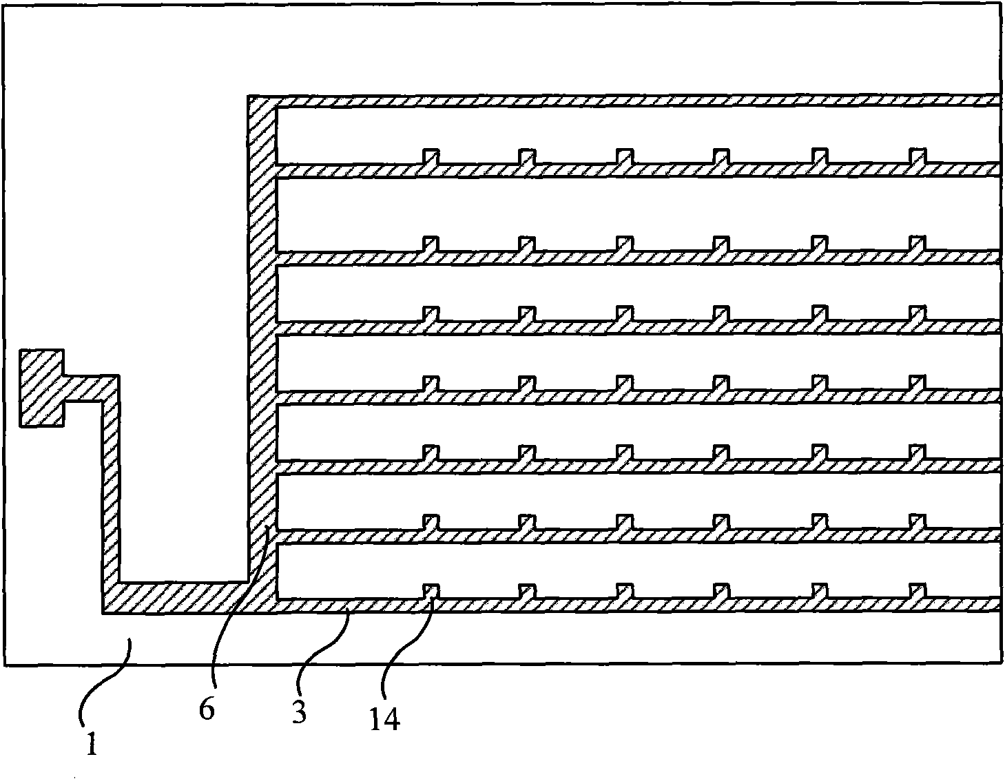
[0037] Figure 5It is a partial top view structural schematic diagram of the array substrate provided by Embodiment 1 of the present invention. The array substrate of this embodiment includes a base substrate 1 , and the base substrate 1 is mostly a glass substrate. A plurality of data lines 2 and gate scan lines 3 intersecting horizontally and vertically are formed on the base substrate 1, surrounding pixel units arranged in a matrix. A TFT switch and a pixel electrode 4 are formed in each pixel unit. In a TFT-LCD, the TFT switch in each pixel unit specifically includes a gate electrode 14 , an active layer 15 , a source electrode 16 and a drain electrode 17 . The gate electrode 14 is connected to the gate scanning line 3 , the source electrode 16 is connected to the data line 2 , and the drain electrode 17 is connected to the pixel electrode 4 . The source electrode 16 and the drain electrode 17 are stacked on the gate electrode 14 through the active layer 15 . The source...

Embodiment 2

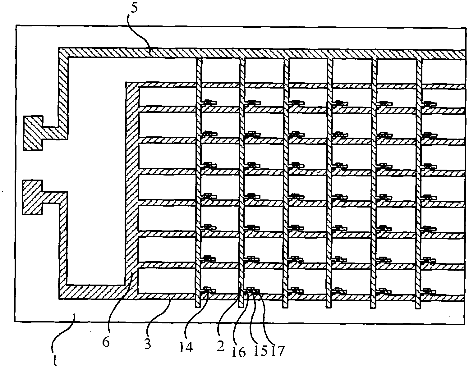
[0050] Figure 8 It is a partial top view structural schematic diagram of the array substrate provided by Embodiment 2 of the present invention. The difference between the array substrate in this embodiment and the first embodiment is that: the data connection line 5 and the pixel electrode 4 are formed in the same layer, and are spaced apart from each other, and the data connection line 5 and each data line 2 pass through the data pass in the first insulating layer. The holes 7 are connected; the gate connection lines 6 are formed in the same layer as the pixel electrodes 4 and are spaced apart from each other, and the gate connection lines 6 and each gate scanning line 3 are connected through gate via holes 8 in the second insulating layer.

[0051] Specifically, when the data connection line 5 and the pixel electrode 4 are formed in the same layer, the first insulating layer only includes the passivation layer, and the data via hole 7 includes the second data via hole penet...

Embodiment 3

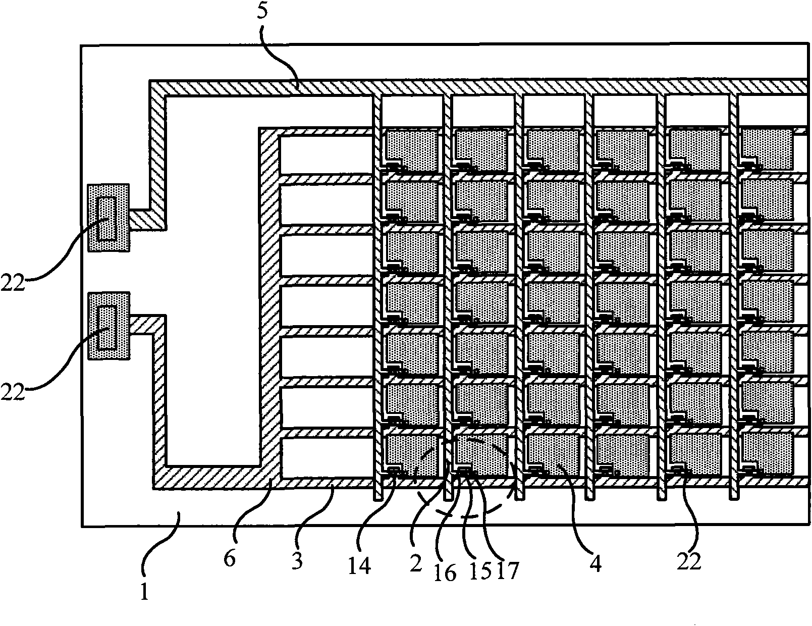
[0054] Figure 9 The partial top view structure schematic diagram of the array substrate provided by the third embodiment of the present invention, the difference between this embodiment and the first embodiment is that the data connection line 5 and the data line 2 are formed on the same layer, and are spaced apart from each other, as shown in Figure 11 Shown is the pattern of the layer where the data line 2 and the data connection line 5 are located. Such as Figure 9 As shown, the data connection line 5 is connected to each data line 2 through the data via hole 7 in the first insulating layer. Such as Figure 10 Shown is the pattern of the layer where the gate scanning line 3 and the gate connecting line 6 are located. The gate connecting line 6 and the gate scanning line 3 are formed in the same layer and are spaced apart from each other. Such as Figure 9 As shown, the gate connecting line 6 is connected to each gate scanning line 3 through the gate via hole 8 in the...


PUM


Abstract

The invention relates an array substrate and a manufacturing method thereof. The array substrate comprises an underlayer substrate; a plurality of data lines and grate scanning lines are transversely and longitudinally crossed on the underlayer substrate to encircle to form pixel units arrayed in a matrix form; TFT (Thin Film Transistor) switches and pixel electrodes are formed in the pixel units; the array substrate also comprise data join lines and grating join lines; and the data join lines are mutually isolated, are formed on the same layer with the data lines, the grating scanning lines or the pixel electrodes, and are connected with all the data lines via data through holes in a first insulation layer; and the grating join lines are mutually isolated, are formed on the same layer with the data lines, the grating scanning lines or the pixel electrodes, and are connected with all the grating scanning lines via grating through holes in a second insulation layer. In the invention, by adopting the technical scheme that the grating scanning lines and the grating join lines, as well as the data lines and the data join lines are arranged at intervals on the same layer or different layers, the signal to noise ratio and the defect relevance ratio of detection signals are improved when defects of the grating scanning lines and the data lines are detected.

Description

technical field [0001] The invention relates to liquid crystal display testing technology, in particular to an array substrate with a testing circuit structure and a manufacturing method thereof. Background technique [0002] With the continuous improvement of thin film transistor liquid crystal display (Thin Film Transistor Liquid Crystal Display, hereinafter referred to as: TFT-LCD) manufacturing technology and the continuous reduction of cost, TFT-LCD has been widely used. The liquid crystal panel is the main display component in TFT-LCD, and is usually formed by pairing a color filter substrate and an array substrate. [0003] A typical structure of an array substrate includes a plurality of data lines and gate scanning lines crossing horizontally and vertically, surrounding pixel units arranged in a matrix. A TFT switch is formed in each pixel unit, and the data line and the pixel electrode are connected through the TFT switch. In order to ensure the normal display of...

Claims


Application Information

Patent Timeline
Patent Type & Authority Applications(China)
IPC IPC(8): G02F1/1362G02F1/1368H01L21/82
Inventor 陈宇鹏郑尧燮
Owner BEIJING BOE OPTOELECTRONCIS TECH CO LTD
Why Eureka
Try Eureka