

Method for establishing space correlation model of technical error in integrated circuit chip
A technology of spatial correlation and process deviation, applied in the direction of electrical digital data processing, special data processing applications, instruments, etc., can solve the problems of not considering the interference of pure random parts and measurement errors, and the accuracy of extraction results will be seriously affected.
- Summary
- Abstract
- Description
- Claims
- Application Information
AI Technical Summary
Problems solved by technology
Method used
Image


Examples
Embodiment Construction
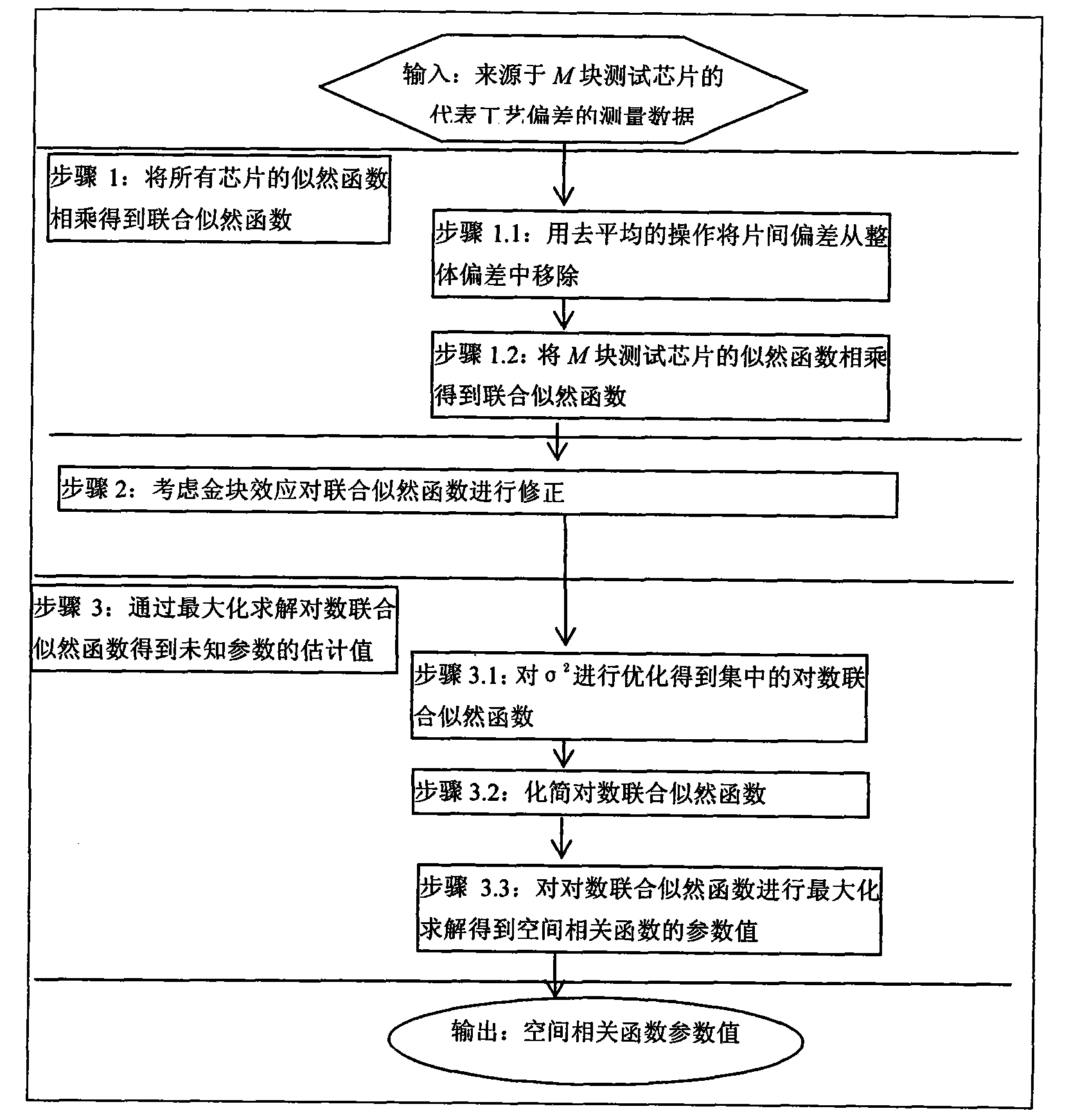
[0085] The present invention is further illustrated below by specific implementation examples:
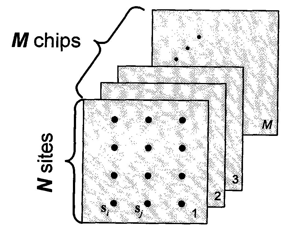
[0086] The present invention utilizes computer simulations to generate pseudo-measurement data. Pseudo-measurement data representing process variation mainly consists of four components: the spatially correlated part of intra-die variation, the purely random part of intra-die variation, the inter-die variation, and the measurement error.
[0087] The spatial correlation part of the intra-chip deviation is the most important component in the measurement data, and its correlation function is the spatial correlation function that reflects the spatial correlation of the intra-chip deviation. This part of the deviation can be simulated by a Gaussian random field [3, 4]. In the implementation example of the present invention, a method based on Cholesky decomposition is used to generate random fields [5]. The specific steps are as follows: First, according to a certain sampling strategy...
PUM
 Abstract
Description
Claims
Application Information