Real-time monitoring method of acceptance test of wafer

A real-time monitoring, wafer technology, applied in semiconductor/solid-state device testing/measurement, electrical components, semiconductor/solid-state device manufacturing, etc. Round and other problems, to reduce losses and avoid scratches

Inactive Publication Date: 2011-03-30
SEMICONDUCTOR MANUFACTURING INTERNATIONAL (BEIJING) CORP +1
View PDF0 Cites 12 Cited by
  • Summary
  • Abstract
  • Description
  • Claims
  • Application Information

AI Technical Summary

Problems solved by technology

[0004] During the test process, the probe points on the wafer used to contact the probes on the probe card are relatively small and closely arranged, and calibration deviation is prone to occur when the wafer image calibration device performs image calibr

Method used


Image

  • Real-time monitoring method of acceptance test of wafer
  • Real-time monitoring method of acceptance test of wafer

Examples


Embodiment Construction

[0022] In order to make the technical features of the present invention more comprehensible, the present invention will be further described below in conjunction with the accompanying drawings and embodiments.

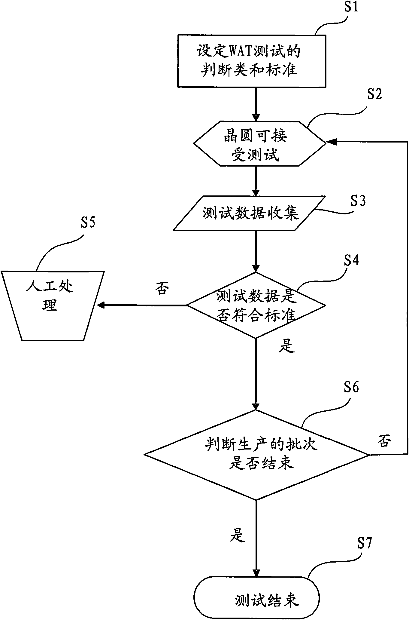
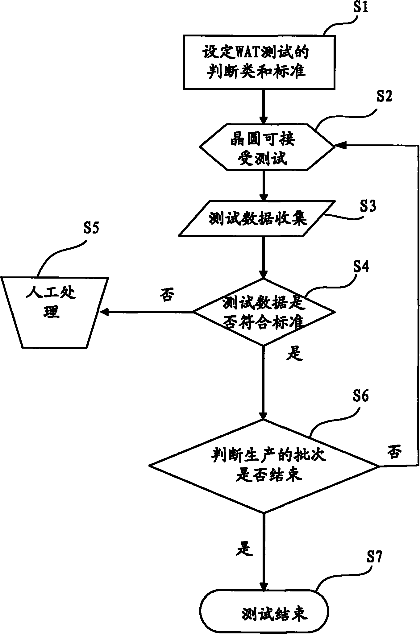
[0023] The real-time monitoring method of the wafer acceptability test of the embodiment of the present invention divides the wafer into several points (site), and the described point is the size that can be exposed by a mask layout. According to the type of product, each site There are several test parameters to be tested, some of which are key parameters, to set the type and judgment standard of the wafer acceptance test; then conduct the wafer acceptance test; then collect and organize the test data obtained from the wafer acceptance test ; Judging according to the type and judgment standard, monitoring the test data, if the judgment is qualified, then continue the test, otherwise, suspend the test and transfer to manual processing.

[0024] The parameters described...


PUM


Abstract

The invention discloses a real-time monitoring method of an acceptance test of a wafer, the wafer is divided into a plurality of points, each point comprises a plurality of test parameters for testing, and part of the parameters are key parameters, and the real-time monitoring method comprises the following steps: setting the type and the judgment standard of the acceptance test of the wafer; carrying out the acceptance test on the wafer; collecting and managing test data obtained by the acceptance test of the wafer; and carrying out judgment according to the type and the judgment standard, monitoring the test data, continuing the test if being judged to be qualified, otherwise, suspending the test and transferring into manual handling. Compared with the prior art, the real-time monitoring method of the acceptance test of the wafer can monitor the data tested by a chip on each wafer, find whether a probe of a probe card is aimed at a probe point on the corresponding chip in time, further avoid the follow-up batch of the chips to be tested from being scratched and reduce the loss.

Description

technical field [0001] The invention relates to an electronic testing method, in particular to a real-time monitoring method for wafer acceptance testing in the semiconductor field. Background technique [0002] Wafer Acceptance Test (WAT: Wafer Acceptance Test) is an electrical test performed before packaging after the wafer (wafer) is manufactured through a complex process, and finally a lattice of bare die (die) is formed on the wafer. , such as parameters such as current, voltage or leakage current of each chip on the wafer are tested. A test system for WAT usually consists of a probe card, a wafer fixture, a wafer image calibration device, and a test machine. [0003] In the process of traditional testing, due to the influence of the calibration deviation of the wafer image calibration device, or the poor contact between the probes on the probe card and the wafer, the ambient temperature or humidity changes around the test machine, the test results and The data is not...

Claims


Application Information

Patent Timeline
IPC IPC(8): H01L21/00H01L21/66
Inventor 孙新光莫保章倪晓昆
Owner SEMICONDUCTOR MANUFACTURING INTERNATIONAL (BEIJING) CORP
Why Eureka
Try Eureka