White-light organic electroluminescent device and preparation method thereof

An electroluminescent device and electroluminescent technology, which are applied in the fields of electro-solid devices, semiconductor/solid-state device manufacturing, electrical components, etc., can solve problems such as affecting the luminous efficiency of devices, and achieve the effects of excellent device performance and excellent color stability.

Inactive Publication Date: 2011-04-06
UNIV OF ELECTRONICS SCI & TECH OF CHINA
View PDF6 Cites 13 Cited by
  • Summary
  • Abstract
  • Description
  • Claims
  • Application Information

AI Technical Summary

Problems solved by technology

For these organic electroluminescent devices with color conversion layer, the spectrum of the device changes with time due to the life of the color conversion layer, and because the color conversion layer affects the light extraction efficiency of the device, it greatly affects the luminous efficiency of the device

Method used


Image

  • White-light organic electroluminescent device and preparation method thereof
  • White-light organic electroluminescent device and preparation method thereof
  • White-light organic electroluminescent device and preparation method thereof

Examples


Embodiment 1

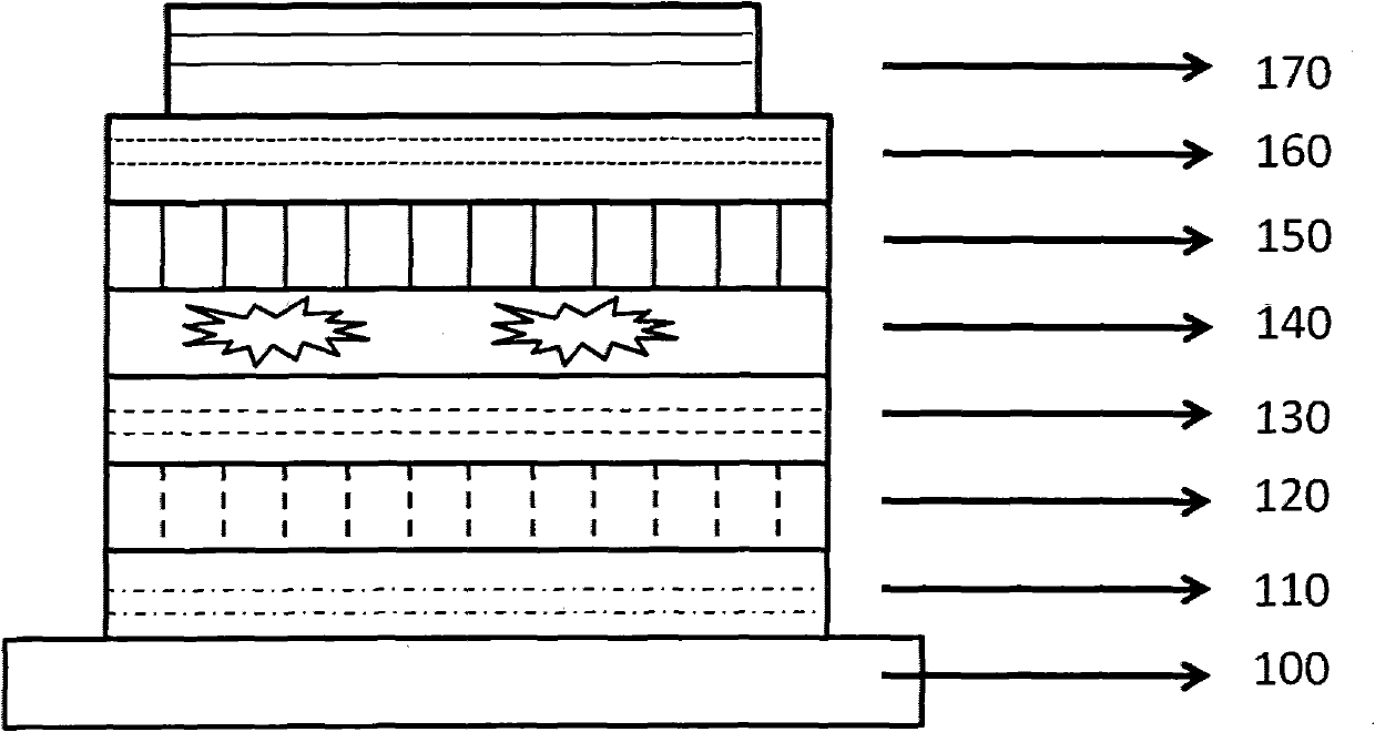
[0067] like figure 1 As shown, the substrate 100 of the device is a glass substrate, the first electrode layer 110 is an anode, 120 is a hole injection layer, 130 is a hole transport layer, the light emitting layer in the structure of the device is 140, and the electron transport layer is 150 , the electron injection layer is 160, and the cathode layer is 170.

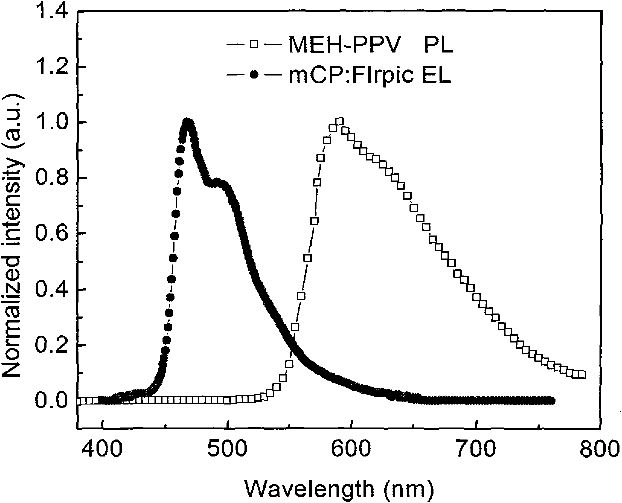
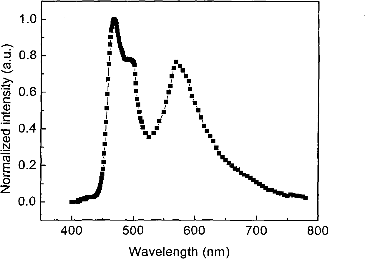
[0068] The material of the hole injection layer of the device is MEH-PPV, the material of the hole transport layer is NPB, the material of the light emitting layer is FIrpic doped with mCP, the material of the electron transport layer is TPBi, and the material of the electron injection is Alq 3 , The cathode layer is made of Mg:Ag alloy. The entire device structure is described as:

[0069] Glass substrate / ITO / MEH-PPV(100nm) / NPB(30nm) / mCP: FIrpic(20nm) / TPBi(20nm) / Alq 3 (30nm) / Mg:Ag(100nm)

[0070] The preparation method is as follows:

[0071] ①Use detergent, ethanol solution and deionized water to ultrasonically ...

Embodiment 2

[0079] like figure 1 As shown, the substrate 100 of the device is a flexible substrate, the first electrode layer 110 is an anode, 120 is a hole injection layer, 130 is a hole transport layer, the light emitting layer in the structure of the device is 140, and the electron transport layer is 150 , the electron injection layer is 160, and the cathode layer is 170.

[0080] The flexible substrate of the device is PET, the material of the hole injection layer is MEH-PPV, the material of the hole transport layer is NPB, the blue phosphorescent material FIrpic doped mCP is selected for the light emitting layer, the material of the electron transport layer is TPBi, and the electron injection material is selected as Alq 3 , The cathode layer is made of Mg:Ag alloy. The entire device structure is described as:

[0081] Flexible substrate / ITO / MEH-PPV(100nm) / NPB(30nm) / mCP: FIrpic(20nm) / TPBi(20nm) / Alq 3 (30am) / Mg:Ag(100nm)

[0082] The preparation method is as follows:

[0083] ①Us...

Embodiment 3

[0091] like figure 1 As shown, the substrate 100 of the device is a flexible substrate, the first electrode layer 110 is a polymer conductive anode, 120 is a hole injection layer, 130 is a hole transport layer, the light emitting layer in the structure of the device is 140, and the electron transport The layer is 150, the electron injection layer is 160, and the cathode layer is 170.

[0092] The polymer conductive anode of the device is PANI, the material of the hole injection layer is MEH-PPV, the material of the hole transport layer is NPB, the blue phosphorescent material FIrpic is doped with mCP for the light emitting layer, the material of the electron transport layer is TPBi, and the electron injection material is selected for Alq 3 , The cathode layer is made of Mg:Ag alloy. The entire device structure is described as:

[0093] Flexible substrate / PANI / MEH-PPV(100nm) / NPB(30nm) / mCP: FIrpic(20nm) / TPBi(20nm) / Alq 3 (30nm) / Mg:Ag(100nm)

[0094] The preparation method is...


PUM


Abstract

The invention discloses a white-light organic electroluminescent device with a supplementary color layer and a preparation method thereof. The organic electroluminescent device comprises a substrate, a first electrode layer positioned on the surface of the substrate, a function layer positioned on the surface of the first electrode layer, and a second electrode formed on the surface of the function layer, wherein the function layer comprises an electron injection layer, an electron transport layer, a luminous layer, a hole transport layer and a hole injection layer; the electroluminescent wavelength of the luminous layer ranges from 380 to 560nm; and the hole injection layer is a layer of organic film with supplementary color function, and comprises a hole injection material with the electroluminescent wavelength between 560 and 780nm. The illumination stability of the organic electroluminescent device effectively is improved effectively, and the preparation process for the device is simplified.

Description

technical field [0001] The invention relates to the technical field of organic optoelectronics in electronic components, in particular to a white light organic electroluminescence device and a preparation method thereof. Background technique [0002] Organic Light-Emitting Device (OLED) is an optoelectronic device that uses organic solid-state semiconductors as light-emitting materials. Its light-emitting mechanism is electroluminescence (EL), so it is also called organic electroluminescence. Light-emitting device (Organic Electroluminescence Device, OLED). Its structure is figure 1 As shown, it includes a substrate 100, an anode electrode 110, a hole injection layer (HIL) 120, a hole transport layer (HTL) 130, an emission layer (EML) 140, and an electron transport layer. A layer (Electron Transport Layer, ETL) 150 , an electron injection layer (Electron Injection Layer, EIL) 160 , and a cathode electrode 170 . When a forward bias voltage is applied to the anode and catho...

Claims


Application Information

Patent Timeline
Patent Type & Authority Applications(China)
IPC IPC(8): H01L51/50H01L51/54H01L51/56
Inventor 于军胜张伟于欣格蒋亚东
Owner UNIV OF ELECTRONICS SCI & TECH OF CHINA
Why Eureka
Try Eureka