Method for preparing slab waveguide laser device in neodymium-doped lutecium vanadate crystal
A strip waveguide and laser device technology, which is applied in the field of optoelectronic device preparation, achieves the effects of high controllability, low cost and strong arbitrariness
- Summary
- Abstract
- Description
- Claims
- Application Information
AI Technical Summary
Problems solved by technology
Method used
Image
Examples
Embodiment 1
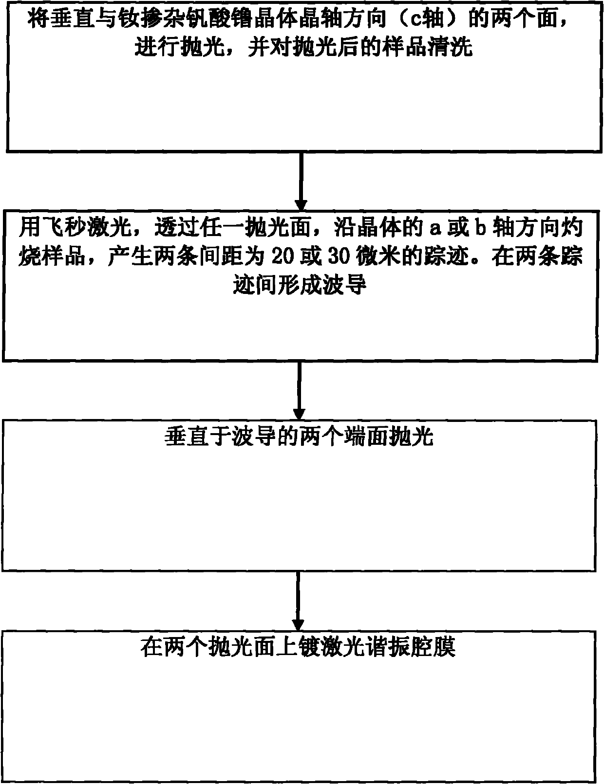
[0014] Embodiment 1: Method for preparing strip waveguide laser device in neodymium-doped lutetium vanadate crystal
[0015] 1) Polishing the two surfaces perpendicular to the crystal axis direction (c-axis) of the neodymium-doped lutetium vanadate crystal (2), and cleaning the polished sample;
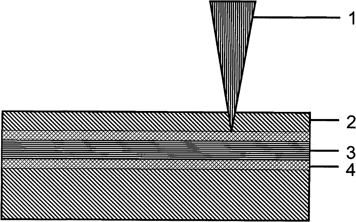
[0016] 2) Use a femtosecond laser (1) to burn the sample along the a-axis direction of the crystal through any polished surface to produce two traces with a distance of 30 microns. A strip waveguide (3) is formed between the two traces. Use a femtosecond laser (1) with a pulse repetition frequency of 200 kHz, an energy of 8 microjoules / pulse, a femtosecond laser with a writing speed of 1 mm / s, a wavelength of 1047 nm, and a pulse width of 350 femtoseconds.
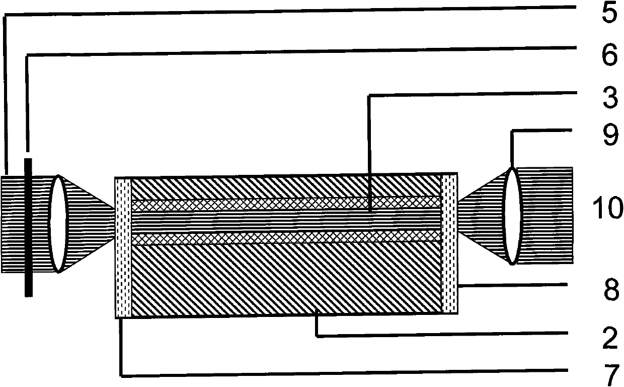
[0017] 3) Polishing the two end faces of the crystal perpendicular to the direction of the strip waveguide.
[0018] 4) Coating the laser cavity film (7, 8) on the polished end face. The resonant cavity film in the direction of...
Embodiment 2
[0020] Embodiment 2: Method for preparing strip waveguide laser device in neodymium-doped lutetium vanadate crystal
[0021] 1) Polishing the two surfaces perpendicular to the crystal axis direction (c-axis) of the neodymium-doped lutetium vanadate crystal (2), and cleaning the polished sample;
[0022] 2) Use a femtosecond laser (1) to burn the sample along the a-axis direction of the crystal through any polished surface to produce two traces with a distance of 30 microns. A strip waveguide (3) is formed between the two traces. Use a femtosecond laser (1) with a pulse repetition frequency of 200 kHz, an energy of 9 microjoules / pulse, a writing speed of 2 mm / s, a wavelength of 1047 nm, and a pulse width of 350 femtoseconds.
[0023] 3) Polishing the two end faces of the crystal perpendicular to the direction of the strip waveguide.
[0024] 4) Coating the laser cavity film (7, 8) on the polished end face. The resonant cavity film in the direction of passing light is require...
PUM
 Abstract
Description
Claims
Application Information
 - R&D Engineer
- R&D Manager
- IP Professional
- Industry Leading Data Capabilities
- Powerful AI technology
- Patent DNA Extraction
Browse by: Latest US Patents, China's latest patents, Technical Efficacy Thesaurus, Application Domain, Technology Topic, Popular Technical Reports.
© 2024 PatSnap. All rights reserved.Legal|Privacy policy|Modern Slavery Act Transparency Statement|Sitemap|About US| Contact US: help@patsnap.com


