Two-dimensional photonic crystal controllable ''AND/OR'' logic gate

A two-dimensional photonic crystal and logic gate technology, applied in the field of optoelectronic information, can solve the problems of unfavorable large-scale all-optical integration, bulky, complex structure of optical logic gate devices, etc., and achieve small size, simple preparation process and simple structure. Effect

Inactive Publication Date: 2011-04-13
SHENZHEN UNIV
View PDF2 Cites 24 Cited by
  • Summary
  • Abstract
  • Description
  • Claims
  • Application Information

AI Technical Summary

Problems solved by technology

[0003] The purpose of the present invention is to address the above-mentioned deficiencies, to provide a two-dimensional photonic crystal controllable "and/or" logic gate that can be logically controlled by all-optical signals. Due to the structure and process characteristics of the two-dimensional photonic crystal itself, it can The functional modules can

Method used


Image

  • Two-dimensional photonic crystal controllable ''AND/OR'' logic gate
  • Two-dimensional photonic crystal controllable ''AND/OR'' logic gate
  • Two-dimensional photonic crystal controllable ''AND/OR'' logic gate

Examples


Embodiment Construction

[0012] The present invention will be further elaborated below according to the drawings and specific embodiments.

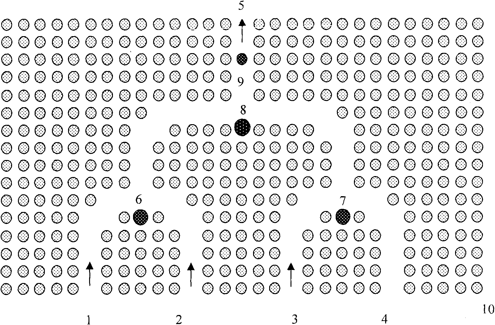
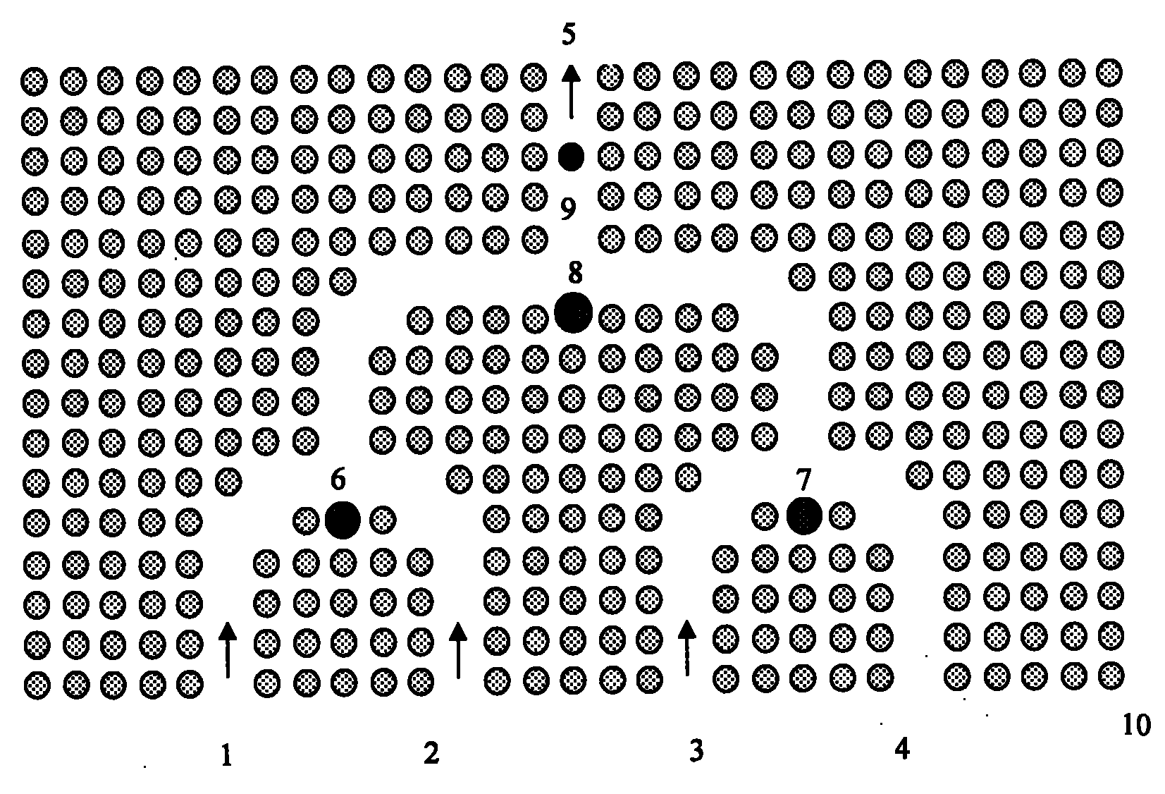
[0013] Such as figure 1 As shown, the two-dimensional photonic crystal controllable AND / OR logic gate structure of the present invention includes four input waveguides 1, input waveguides 2, input waveguides 3, input waveguides 4 and one output waveguide 5. The input waveguide 1, input waveguide 2, input waveguide 3, input waveguide 4 and output waveguide 5 are all formed by removing some rows of two-dimensional photonic crystal dielectric rods 10 in the two-dimensional photonic crystal. Mirror symmetrical distribution. The intersection of input waveguide 1 and input waveguide 2 is provided with a nonlinear dielectric rod 6 as a coupling area, and the intersection of input waveguide 3 and input waveguide 4 is provided with a nonlinear dielectric rod 7 as a coupling area, and then input waveguides 1 and 2 and input waveguide 3 The intersection of , 4 is provided...


PUM


Abstract

The invention relates to a two-dimensional photonic crystal controllable ''AND/OR'' logic gate which comprises four input waveguides and an output waveguide, wherein one input waveguide is used for inputting a control signal; one input waveguide is an idle waveguide; and the other two input waveguides are signal input waveguides. The logic gate is distributed in a mirror symmetry way with a network center axial line of a linear defect waveguide; the symmetrical center position of the intersection of every two input waveguides of the logic gate is provided with a nonlinear dielectric rods as a coupling modulating zone for modulating signal power leading to the next stage of output waveguide; and a nonlinear dielectric rod is arranged on the output waveguide of the logic gate away from the third dielectric rod of the coupling modulating zone. The controllable AND/OR logic gate can be used for logic control of an optical signal by using an all-optical signal, and has the characteristics of small volume, simple structure and high response speed. In addition, all-optical modules of different functions can be manufactured on the same chip so as to be suitable for large-scale optoelectronic integration.

Description

technical field [0001] The invention relates to the field of optoelectronic information technology, in particular to a two-dimensional photonic crystal controllable "and / OR" logic gate. Background technique [0002] All-optical logic devices are devices that directly use photons to realize logic functions such as "and", "or", and "not". An important device in all-optical communication. Most of the optical logic gate devices that have been proposed so far require electro-optic control, or have a single logic function, or use interferometers, such as Mach-Zehnder interferometer (patent No. 200620115693.X), Sagnac interferometer and other systems (patent No. 200810044878 .X) and so on, the structure is complex and bulky, which is not conducive to large-scale all-optical integration. Contents of the invention [0003] The purpose of the present invention is to address the above-mentioned deficiencies, to provide a two-dimensional photonic crystal controllable "and / or" logi...

Claims


Application Information

Patent Timeline
IPC IPC(8): G02F3/00G02B6/122
Inventor 欧阳征标许桂雯刘远常
Owner SHENZHEN UNIV
Why Eureka
Try Eureka