Solution concentration monitoring method

A solution concentration, solution technology, applied in measuring devices, instruments, scientific instruments, etc., can solve the problem of high cost of monitoring solution concentration

Inactive Publication Date: 2011-04-20
SEMICONDUCTOR MANUFACTURING INTERNATIONAL (BEIJING) CORP +1
View PDF4 Cites 1 Cited by
  • Summary
  • Abstract
  • Description
  • Claims
  • Application Information

AI Technical Summary

Problems solved by technology

[0005] In order to solve the problem of relatively high cost of monitoring solution concentration in the prior art, the present invention provides a method for monitoring solution concentration, which can monitor whether the concentration of the solution exceeds the standard at a very low cost

Method used


Image

  • Solution concentration monitoring method
  • Solution concentration monitoring method

Examples


Embodiment Construction

[0032] In order to make the content and protection scope of the present invention clearer and easier to understand, the content of the present invention will be described in detail below in conjunction with the accompanying drawings.

[0033] The inventor found a new method to simulate and monitor the concentration of SC1 through multiple experiments and data analysis and summarized the rules. The experimental results confirmed that the etching rate of polysilicon is different for different concentrations of SC1, and within a certain concentration range The etch rate is relatively stable. So we take advantage of this feature to simulate the concentration of SC1 by testing the etching rate of SC1 with a polysilicon control chip. This is completely different from the professional equipment for monitoring SC1 concentration commonly used in the industry at present.

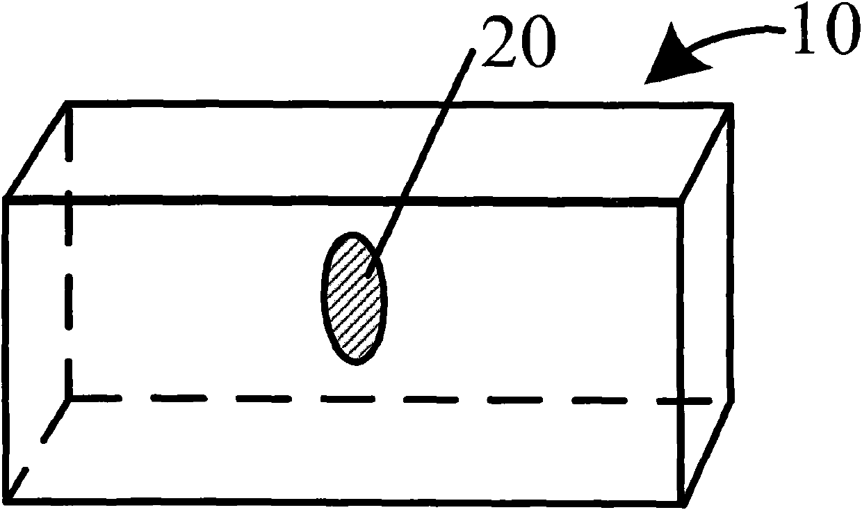
[0034] figure 1 It is a schematic diagram of soaking the polysilicon control chip into the solution. figure 1 In...


PUM

PropertyMeasurementUnit
thicknessaaaaaaaaaa

Abstract

The invention provides a solution concentration monitoring method. The concentration of a solution is monitored through monitoring the reaction rate of a polysilicon control wafer by utilizing the characteristics that the reaction rates of the polysilicon control wafer and the solution are stable when the solution concentration is in a certain range. Compared with methods in the prior art, the solution concentration monitoring method of the invention greatly decreases the cost.

Description

technical field [0001] The invention relates to the technical field of semiconductor testing, in particular to a method for monitoring solution concentration. Background technique [0002] In the chip manufacturing process, the mixed solution (SC1) cleaning of ammonia water, peroxide water and deionized water is the most commonly used cleaning method to remove dust particles on the chip surface. Changes in the concentration of SC1 will affect the performance of the chip. At present, various manufacturers mainly use professional equipment for monitoring the concentration of SC1, that is, the online detection equipment of HORIBA Company to monitor the concentration of SC1 online. [0003] Since HORIBA’s online testing equipment is relatively expensive, about US$100,000 each, and each SC1 acid tank must be controlled by an online testing equipment, this greatly increases the cost of the machine. It also increases the manufacturing cost of the chip. [0004] Therefore, how to ...

Claims


Application Information

Patent Timeline
Patent Type & Authority Applications(China)
IPC IPC(8): G01N33/00
Inventor 刘卫魏广生
Owner SEMICONDUCTOR MANUFACTURING INTERNATIONAL (BEIJING) CORP
Why Eureka
Try Eureka