Unlock instant, AI-driven research and patent intelligence for your innovation.

TFT (Thin Film Transistor) array structure and manufacturing method thereof

A technology of an array structure and a manufacturing method, applied in the field of TFT array structure and its manufacturing, can solve the problems of poor capacitor storage capacity and small storage capacitor capacitance value, etc.

Active Publication Date: 2011-04-20
SHANGHAI TIANMA MICRO ELECTRONICS CO LTD
View PDF1 Cites 1 Cited by
  • Summary
  • Abstract
  • Description
  • Claims
  • Application Information

AI Technical Summary

Problems solved by technology

[0008] The purpose of the present invention is to provide a TFT array structure and its manufacturing method, to solve the problem of small storage capacitor capacitance and poor capacitance storage capacity in the TFT array structure in the prior art

Method used


Image

  • TFT (Thin Film Transistor) array structure and manufacturing method thereof
  • TFT (Thin Film Transistor) array structure and manufacturing method thereof
  • TFT (Thin Film Transistor) array structure and manufacturing method thereof

Examples


no. 1 example

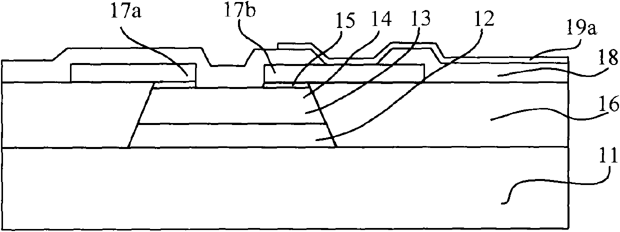
[0099] In one embodiment of the present invention, a kind of manufacturing method of TFT array structure is provided, such as Image 6 shown, including steps:

[0100] S101, providing a substrate, the substrate has a first region and a second region;

[0101] S102, sequentially forming a gate electrode metal layer, a gate electrode insulating layer, a semiconductor layer and an ohmic contact layer on the substrate;

[0102] S103, using a mask plate to define a photoresist pattern;

[0103] S104, using the photoresist pattern as a mask, removing the ohmic contact layer, semiconductor layer, gate electrode insulating layer, and gate electrode metal layer on areas other than the first area and the second area, and exposing the the substrate;

[0104] S105, forming a first insulating layer on a region of the substrate other than the first region and the second region;

[0105] S106, forming a source-drain electrode metal layer on the first insulating layer and the ohmic contac...

no. 2 example

[0165] In one embodiment of the present invention, a kind of manufacturing method of TFT array structure is provided, such as Figure 21 shown, including steps:

[0166] S201, providing a substrate, the substrate has a first region and a second region;

[0167] S202, sequentially forming a gate electrode metal layer, a gate electrode insulating layer, a semiconductor layer and an ohmic contact layer on the substrate;

[0168] S203, using a half-gray mask to define a photoresist pattern;

[0169] S204, using the photoresist pattern as a mask, removing part of the ohmic contact layer, semiconductor layer, gate electrode insulating layer, and gate electrode metal layer; leaving the ohmic contact layer, semiconductor layer, and gate electrode on the first region an insulating layer and a gate electrode metal layer; leaving the gate electrode insulating layer and the gate electrode metal layer on the second region;

[0170] S205, forming a first insulating layer on the periphery...


PUM

PropertyMeasurementUnit
Thicknessaaaaaaaaaa
Thicknessaaaaaaaaaa
Thicknessaaaaaaaaaa

Abstract

The invention relates to a TFT (Thin Film Transistor) array structure and a manufacturing method thereof. The TFT array structure comprises a substrate, a gate electrode metal layer, a gate electrode insulating layer, a semiconductor layer, an ohmic contact layer, a first insulating layer, a source electrode metal layer, a drain electrode metal layer, a channel between the source electrode metal layer and the drain electrode metal layer and a pixel electrode which covers the gate electrode insulating layer and is connected with the drain electrode metal layer through a through hole, wherein the pixel electrode and the gate electrode metal layer forms two poles of a storage capacitor, and the storage medium of the storage capacitor is a single-layer structure of a double-layer structure. Compared with the prior art, the storage capacitor has larger capacitance storage capacity.

Description

technical field [0001] The invention relates to display technology, in particular to a TFT array structure and a manufacturing method thereof. Background technique [0002] Due to the advantages of lightness, thinness, small footprint, low power consumption, and low radiation, flat panel display devices are widely used in various data processing devices, such as televisions, notebook computers, mobile phones, and personal digital assistants. With the continuous development of the electronic industry, the performance of flat panel display devices is getting higher and higher. [0003] Taking a common thin film transistor liquid crystal display (Thin Film Transistor Liquid Crystal Display, TFT-LCD) as an example, it is a kind of active matrix liquid crystal display. The main feature of TFT-LCD is that each pixel is equipped with a semiconductor switching device, and each pixel is an independent transistor isolated from each other. Since each pixel can be directly controlled b...

Claims


Application Information

Patent Timeline
IPC IPC(8): G02F1/1362G02F1/1368H01L27/02H01L21/82G03F7/00
Inventor 黄贤军
Owner SHANGHAI TIANMA MICRO ELECTRONICS CO LTD
Features
  • R&D
  • Intellectual Property
  • Life Sciences
  • Materials
  • Tech Scout
  • Unparalleled Data Quality
  • Higher Quality Content
  • 60% Fewer Hallucinations
Learn More