Doping method

A light doping and heavy doping technology, applied in the field of doping, can solve the problems of large performance differences of semiconductor devices and relatively large performance differences of semiconductor devices, and achieve the effect of reducing performance differences

Active Publication Date: 2011-04-20
SEMICON MFG INT (SHANGHAI) CORP
View PDF0 Cites 10 Cited by
  • Summary
  • Abstract
  • Description
  • Claims
  • Application Information

AI Technical Summary

Problems solved by technology

[0006] The above steps 1 and 3 all involve the ion implantation process. Theoretically, when performing ion implantation, the ion beam emitting device should be adjusted in advance, and the ion beam emitted by the ion beam emitting device should be perpendicular to the substrate surface, so that It can be guaranteed that the ion concentrations of the lightly doped drain and the lightly doped source formed in step three are equal, but in practical applications, due to errors, the ion beam emitted by the ion beam emitting device may not be vertical on the surface of the substrate, and because there are differences in the performance of the ion beam emitting devices of different machines, this may cause the angles of the ion beams emitted by the ion beam emitting devices of different machines to be different. For the light doping of batches of semiconductor devices, the same batch of semiconductor devices is generally divided into several groups, and several groups are lightly doped on different machines at the same time, because the ions emitted by the ion beam emitting devices of different machines The angles of the beams are different, which will cause a large difference in the performance of the same batch of semiconductor devices. Moreover, even if the same batch of semiconductor devices is lightly doped on the same machine, due to the influence of temperature or other environmental factors, there will be The performance difference of the same batch of semiconductor devices is relatively large
Similarly, for different batches of devices, the angles of the ion beams emitted by the ion beam emitting device of the machine are also different, which will cause a large difference in the performance of different batches of semiconductor devices.

Method used


Image

  • Doping method
  • Doping method
  • Doping method

Examples


Embodiment Construction

[0038] In order to make the object, technical solution and advantages of the present invention clearer, the present invention will be further described in detail below with reference to the accompanying drawings and examples.
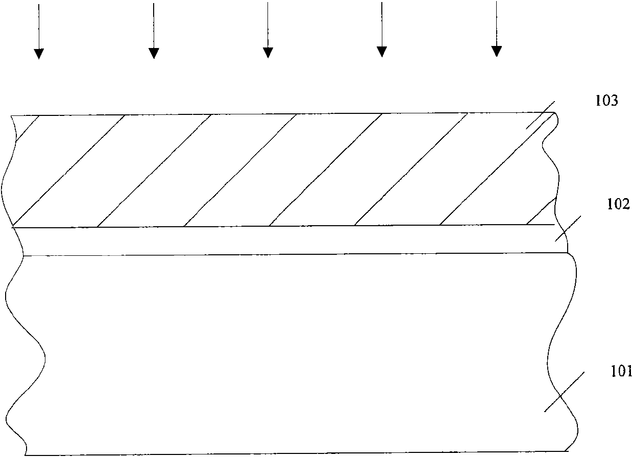
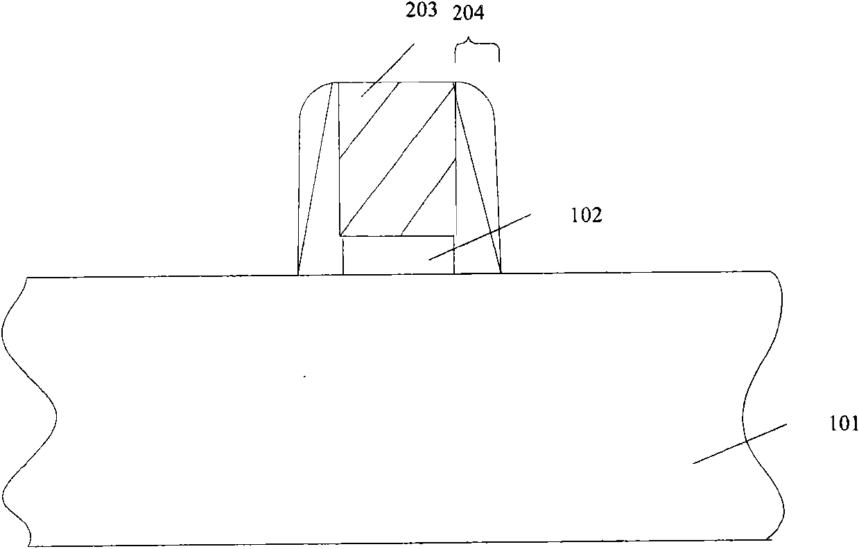
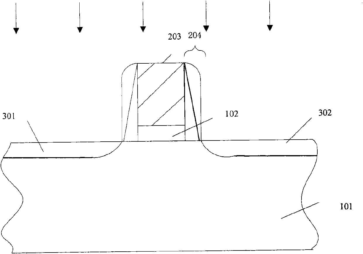
[0039] The core idea of ​​the present invention is: when lightly doping or heavily doping the substrates on both sides of the grid, firstly adjust the angle of the ion beam, and keep a fixed angle between the ion beam and the vertical direction of the substrate surface, Use half of the preset ion implantation dose to lightly or heavily dope the substrates on both sides of the gate, then rotate the wafer 180 degrees in the horizontal direction, and use half of the preset ion implantation dose to do the gate again. Lightly or heavily doped the substrates on both sides of the electrode, and finally form a lightly doped drain and a lightly doped source, or a drain and a source, or first adjust the angle of the ion beam and make the ion beam and The vertical...


PUM


Abstract

The invention discloses a doping method. The method comprises the following steps of: forming a grid electrode structure on a semiconductor substrate; forming side wall layers on the two sides of the grid electrode structure; adjusting an angle of an ion beam and keeping a fixed included angle between the ion beam and the vertical direction of the surface of the substrate; lightly or heavily doping the substrates on the two sides of a grid electrode by using half the preset ion injection dosage; turning a wafer for 180 degrees in the horizontal direction; and lightly or heavily doping the substrates on the two sides of the grid electrode by using half the preset ion injection dosage to form a lightly doped drain electrode and a lightly doped source electrode or drain electrode and source electrode. By the method, the performance difference of a semiconductor device can be reduced.

Description

technical field [0001] The invention relates to the field of semiconductor manufacturing, in particular to a doping method. Background technique [0002] With the wide application of electronic equipment, the manufacturing process of semiconductors has developed rapidly. In the manufacturing process of semiconductors, light doping processes are involved. Doping is performed to form a lightly doped drain and a lightly doped source. Figure 1 ~ Figure 3 It is a process sectional structure diagram of a light doping method in the prior art, and the method includes the following steps: [0003] Step one, see figure 1 , provide a wafer, form the gate oxide layer 102 and the polysilicon layer 103 on the substrate 101 of the wafer, and adopt the ion implantation process to dope the polysilicon layer 103, the dose of ion implantation is 1×10 15 / cm 2 up to 6×10 15 / cm 2 . [0004] Step two, see figure 2 For the polysilicon layer 103 and the gate oxide layer 102, the gate 203...

Claims


Application Information

Patent Timeline
Patent Type & Authority Applications(China)
IPC IPC(8): H01L21/336H01L21/265
Inventor 神兆旭居建华
Owner SEMICON MFG INT (SHANGHAI) CORP
Why Eureka
Try Eureka