Image sensor and manufacturing method of transistor

A technology of image sensor and manufacturing method, which is applied in the direction of transistor, semiconductor/solid-state device manufacturing, semiconductor device, etc., and can solve the problems of image quality reduction, large flicker noise of voltage signal, obvious flicker noise, etc.

Active Publication Date: 2012-10-03
GALAXYCORE SHANGHAI
View PDF5 Cites 5 Cited by
  • Summary
  • Abstract
  • Description
  • Claims
  • Application Information

AI Technical Summary

Problems solved by technology

[0004] However, the voltage signal output by traditional CMOS image sensors often has a large flicker noise, especially when the light is weak, this flicker noise is more obvious
Flicker noise in voltage signals can significantly degrade image quality

Method used


Image

  • Image sensor and manufacturing method of transistor
  • Image sensor and manufacturing method of transistor
  • Image sensor and manufacturing method of transistor

Examples


Embodiment Construction

[0028] The making and using of the embodiments are discussed in detail below. It should be understood, however, that the specific embodiments discussed are merely illustrative of specific ways to make and use the invention, and do not limit the scope of the invention.

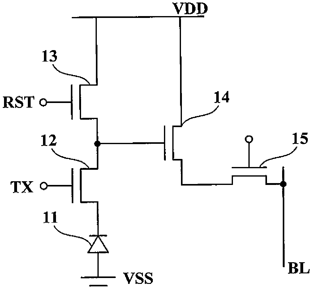
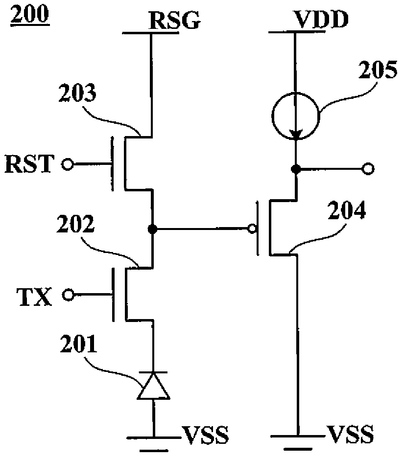
[0029] refer to figure 2 , shows an image sensor 200 according to an embodiment of the present invention, the image sensor 200 includes a pixel array, and each pixel unit in the pixel array includes: a photodiode 201 for sensing light intensity changes to generate corresponding image charges signal; a transfer transistor 202 for transferring the image charge signal; and a source follower transistor 204 for generating a voltage signal based on the transferred image charge signal, wherein the source follower transistor 204 is a junction field effect transistor.

[0030]It should be noted that, in some examples, multiple pixel units in the pixel array may have one source follower transistor 204, for example, two...


PUM


Abstract

The invention discloses an image sensor and a manufacturing method of a transistor. The image sensor comprises a pixel array. One or a plurality of pixel units of the pixel array respectively comprise one source following transistor. Each source following transistor is a junction type field effect transistor and comprises a first conduction type substrate, a second conduction type well, a second conduction type deposition doped layer, a first conduction type source region, a first conduction type drain region and a first conduction type doped layer, wherein the second conduction type well is positioned in the first conduction type substrate; the second conduction type deposition doped layer is positioned outside the surface of the first conduction type substrate and at least part of the second conduction type deposition doped layer is positioned on the second conduction type well; the first conduction type source region is positioned in the second conduction type well; the first conduction type drain region is positioned in the first conduction type substrate and/or the second conduction type well; at least part of the first conduction type doped layer is positioned between the second conduction type well and the second conduction type deposition doped layer so as to ensure the first conduction type source region to be electrically connected with the first conduction type drain region; and PN nodes are respectively formed between the first conduction type doped layer and the second conduction type well and between the first conduction type doped layer and the second conduction type deposition doped layer.

Description

technical field [0001] The present invention relates to the technical field of semiconductors, and more specifically, the present invention relates to an image sensor and a method for manufacturing a transistor. Background technique [0002] Conventional image sensors can generally be classified into two categories: charge coupled device (Charge Coupled Device, CCD) image sensors and complementary metal oxide semiconductor (CMOS) image sensors. Among them, the CMOS image sensor has the advantages of small size, low power consumption, and low production cost. Therefore, the CMOS image sensor is easy to be integrated in portable electronic devices such as mobile phones, notebook computers, and tablet computers, as a camera module that provides digital imaging functions. use. [0003] CMOS image sensors usually use a 3T or 4T pixel structure. figure 1 That is, a 4T pixel structure of a conventional CMOS image sensor is shown, including a photodiode 11 , a transfer transistor ...

Claims


Application Information

Patent Timeline
Patent Type & Authority Applications(China)
IPC IPC(8): H01L27/146H01L29/808H01L21/337
CPCH01L27/146H01L29/808H01L27/14612H01L27/14616
Inventor 赵立新李文强蒋珂玮
Owner GALAXYCORE SHANGHAI
Why Eureka
Try Eureka