TFT-LCD array substrate and manufacturing, detecting and driving methods thereof

A technology of an array substrate and a driving method, which is applied in the field of liquid crystal displays, can solve problems such as easy polarization of liquid crystal molecules, insignificant effects, and residual images, and achieve the effects of simple structure of detection equipment, clear results, and improved yield rate

Active Publication Date: 2011-04-27
BOE TECH GRP CO LTD +1
View PDF5 Cites 22 Cited by
  • Summary
  • Abstract
  • Description
  • Claims
  • Application Information

AI Technical Summary

Problems solved by technology

Since TFT-LCD is a steady-state mode (Hold-Type) display method, there may be charge accumulation in the alignment layer or other microstructures on both sides of the liquid crystal, and the accumulated charge will generate an additional potential difference between the pixel electrode and the common electrode. The additional potential difference will also deflect the liquid crystal when no data signal is applied, resulting in an optical rotation effect and causing image sticking
In addition, when the same screen is displayed for a long time, the liquid crystal molecules are easily polarized, and the polarized liquid crystal molecules will also have an optical rotation effect, causing image sticking.
At present, the existing technology usually adopts the method of diversification of materials to overcome the afterimage defect, but the effect is not significant

Method used


Image

  • TFT-LCD array substrate and manufacturing, detecting and driving methods thereof
  • TFT-LCD array substrate and manufacturing, detecting and driving methods thereof
  • TFT-LCD array substrate and manufacturing, detecting and driving methods thereof

Examples


Embodiment Construction

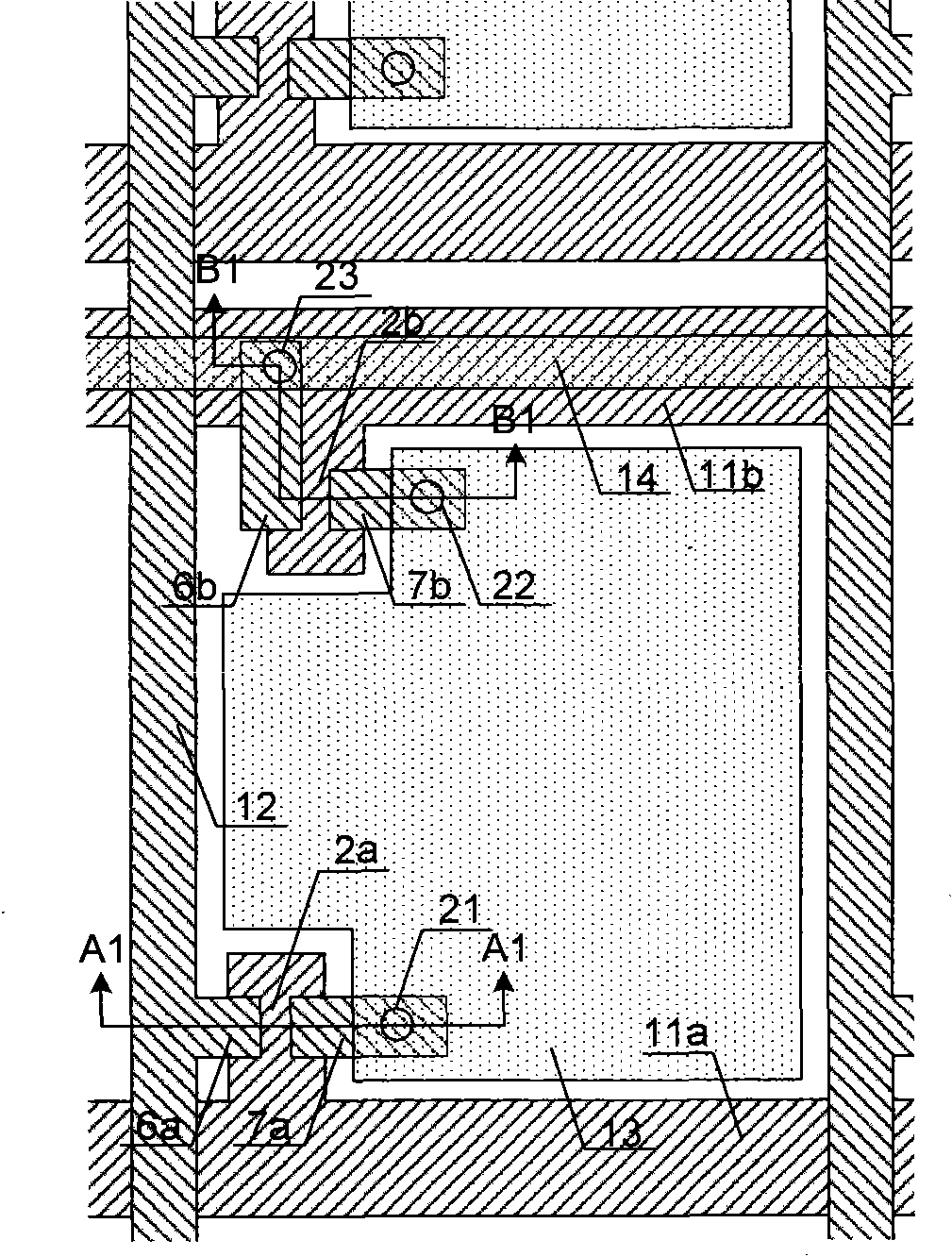
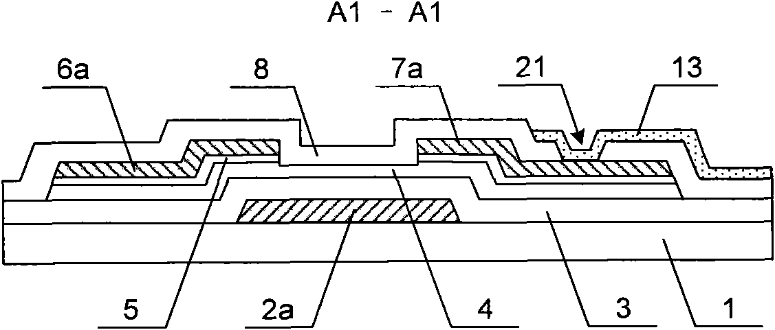
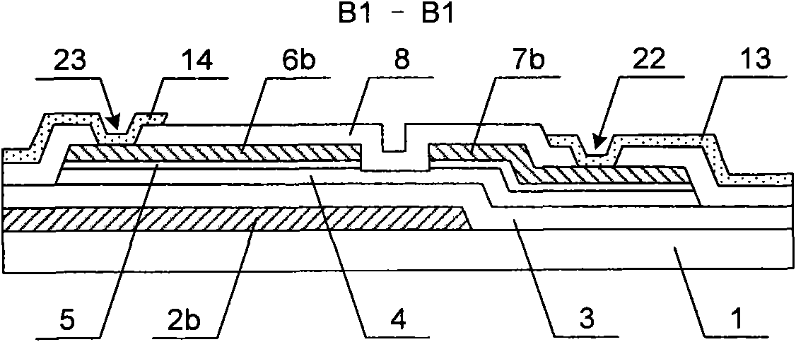
[0046] The technical solutions of the present invention will be described in further detail below with reference to the accompanying drawings and embodiments. The film thicknesses and area sizes and shapes of the various layers in the drawings do not reflect the true proportions of the TFT-LCD array substrate, but are only intended to schematically illustrate the contents of the present invention.

[0047] figure 1 It is a plan view of the TFT-LCD array substrate of the present invention, reflecting the structure of a pixel region, figure 2 for figure 1 The cross-sectional view of A1-A1 in the middle, image 3 for figure 1 Sectional view of B1-B1 direction in the middle. Such as Figure 1 ~ Figure 3 As shown, the main structure of the TFT-LCD array substrate of the present invention includes the first gate line 11a, the second gate line 11b, the data line 12 and the detection line 14 formed on the substrate, the first gate line 11a and the second gate line 11b The adjac...


PUM


Abstract

The invention relates to a thin film transistor-liquid crystal display (TFT-LCD) array substrate and manufacturing, detecting and driving methods thereof. The TFT-LCD array substrate comprises a first grid line, a data line, a pixel electrode and a first thin film transistor which are formed on the substrate, wherein the first thin film transistor is used for controlling the data line to provide data voltage for the pixel electrode; the TFT-LCD array substrate also comprises a second grid line, a detecting line and a second thin film transistor; the second thin film transistor comprises a second grid electrode, a second source electrode and a second drain electrode; the second grid electrode is connected with the second grid line; the second source electrode is connected with the detection line; and the second drain electrode is connected with the pixel electrode. By arranging the second grid line, the detecting line and the second thin film transistor, on one hand, whether the thin film transistor is not good is detected and the characteristic of the thin film transistor is detected in an electrochemical mode; and on the other hand, the residual image defect is effectively overcome, the yield is improved and the production cost is reduced.

Description

technical field [0001] The invention relates to a liquid crystal display, a manufacturing method, a testing method and a driving method of the liquid crystal display, in particular to a TFT-LCD array substrate and a manufacturing, testing and driving method thereof. Background technique [0002] The main structure of a Thin Film Transistor Liquid Crystal Display (TFT-LCD) includes an array substrate and a color filter substrate that are boxed together and liquid crystals are sandwiched between them. The array substrate is formed with gate lines, data lines and the following Thin film transistors and pixel electrodes arranged in a matrix, black matrix, color resin and common electrodes are formed on the color filter substrate, and the liquid crystal molecules are deflected by controlling the voltage difference between the pixel electrodes of the array substrate and the common electrodes of the color filter substrate, and the liquid crystal molecules The different deflection a...

Claims


Application Information

Patent Timeline
Patent Type & Authority Applications(China)
IPC IPC(8): G02F1/1362G02F1/1368H01L21/82G09G3/36
CPCG02F1/1309G09G2310/0262G09G2320/0204G02F2001/136254G02F1/136286G09G2300/0443G02F2001/133397G09G3/3648G09G2320/0257G09G2300/0426G02F1/13624G09G3/3659G09G3/367G09G3/3696G02F1/133397G02F1/136254
Inventor 曹昆李于华
Owner BOE TECH GRP CO LTD
Why Eureka
Try Eureka