

Detection method of degree of damage of plasma
A technology of damage degree and plasma, which is applied in the direction of semiconductor/solid-state device testing/measurement, measuring devices, and measuring electrical variables, etc., can solve problems such as complicated procedures, increased detection costs, and low detection efficiency, so as to improve detection efficiency and reduce The cost of testing and the effect of simplifying testing procedures
- Summary
- Abstract
- Description
- Claims
- Application Information
AI Technical Summary
Problems solved by technology
Method used
Image

Examples
Embodiment Construction
[0040] The method of the present invention provides a detection method for the degree of plasma damage, and only a part of the chips are extracted for the threshold voltage drift test, which reduces the detection cost; the leakage current is used as the detection standard, which can quickly detect plasma damage and improve detection efficiency , can carry out online real-time detection; no need to apply forced voltage, and will not cause damage to the chip.
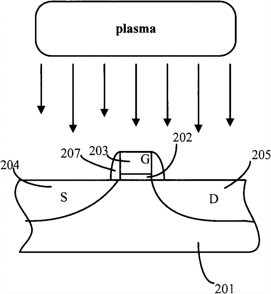
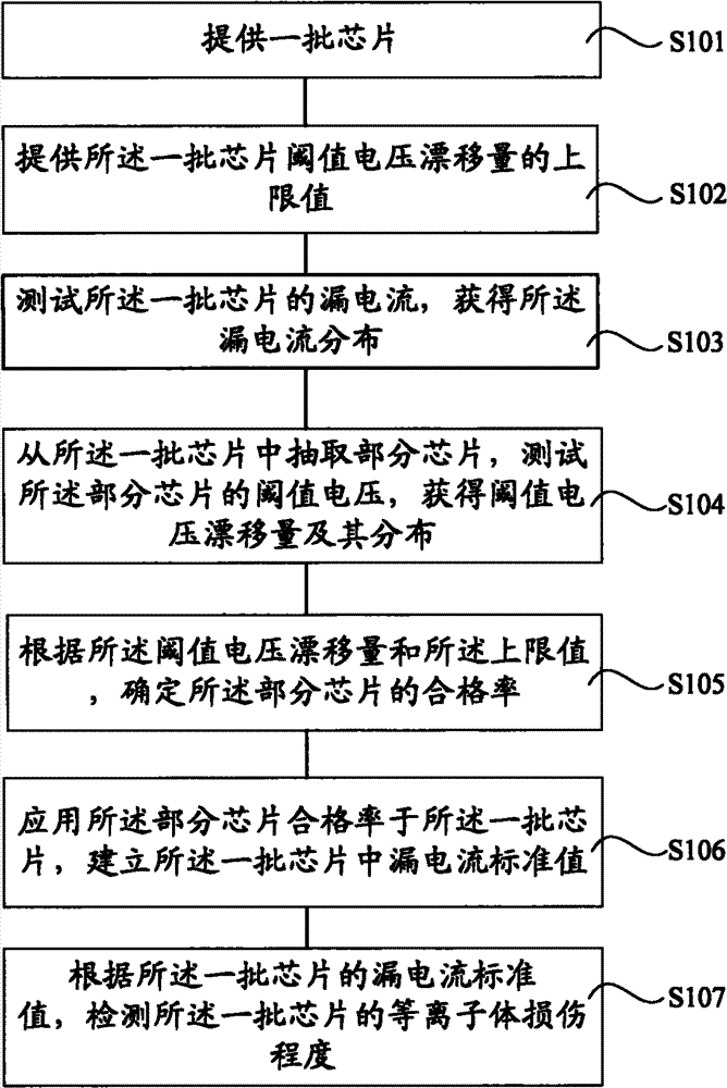
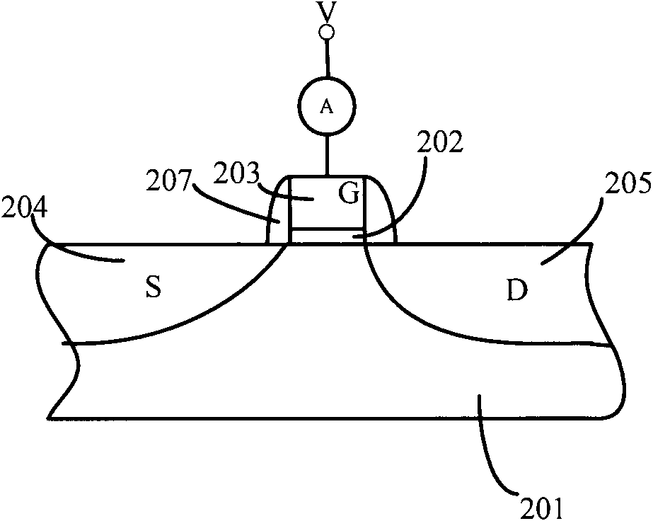
[0041] figure 2 It is a schematic flow chart of the method for detecting the degree of plasma damage of the present invention. Such as figure 2 shown, including:
[0042] Execute step S101 to provide a batch of chips;
[0043] Execute step S102, providing the upper limit value of threshold voltage drift of the batch of chips;
[0044] Execute step S103, test the leakage current of the batch of chips, and obtain the leakage current distribution;
[0045] Execute step S104, extract some chips from the batch of chips,...
PUM
 Abstract
Description
Claims
Application Information