Manufacturing method of semiconductor device

A manufacturing method and semiconductor technology, applied in the direction of semiconductor devices, electrical solid devices, electrical components, etc., can solve problems such as slow program, program failure, and retention problems, and achieve the effect of improving performance and reliability

Active Publication Date: 2017-12-05
SEMICON MFG INT (SHANGHAI) CORP +1
View PDF6 Cites 2 Cited by
  • Summary
  • Abstract
  • Description
  • Claims
  • Application Information

AI Technical Summary

Problems solved by technology

Typically, the floating gate profile is very vertical, and the sidewalls of the floating gate are easily damaged during etch and wet processes, which can lead to retention issues, slow processes, or even process failures

Method used


Image

  • Manufacturing method of semiconductor device
  • Manufacturing method of semiconductor device
  • Manufacturing method of semiconductor device

Examples


Embodiment 1

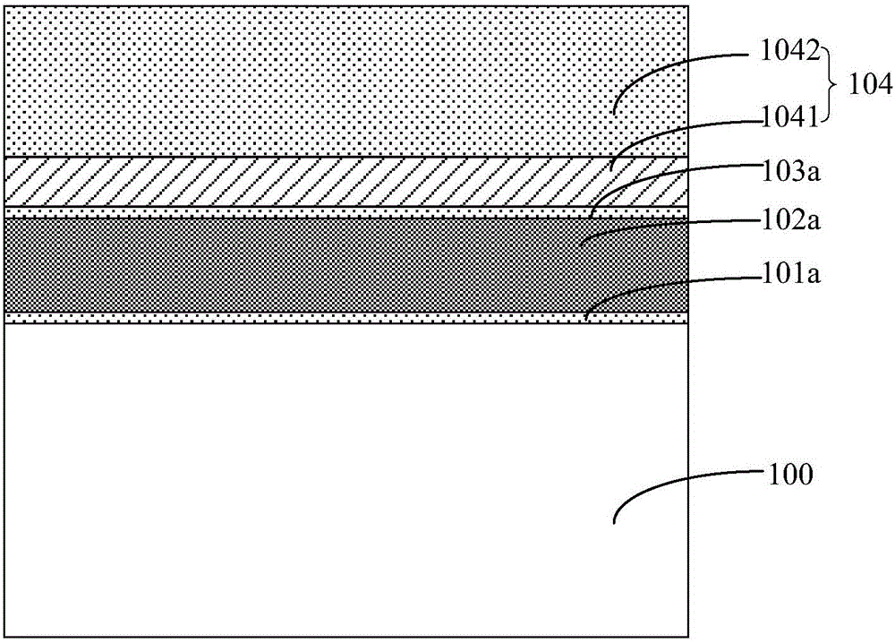
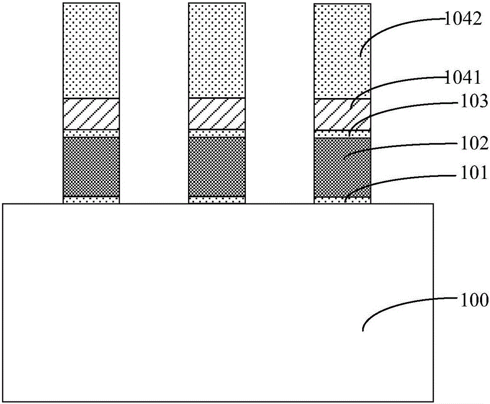
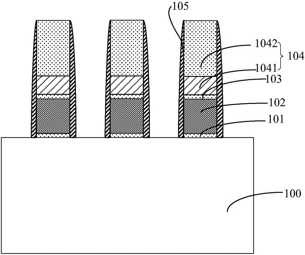
[0041] Below, refer to Figure 1A to Figure 1I The manufacturing method of the semiconductor device of the present invention is described in detail. Figure 1A to Figure 1I It shows a schematic cross-sectional view of a structure obtained by sequentially implementing a method for fabricating a semiconductor device according to an embodiment of the present invention;

[0042] First, if Figure 1A As shown, a semiconductor substrate 100 is provided, and a tunnel oxide layer 101 , a floating gate material layer 102 a , a buffer layer 103 , and a hard mask layer 104 are sequentially deposited and formed on the semiconductor substrate 100 .

[0043] Specifically, the semiconductor substrate 100 may be at least one of the materials mentioned below: silicon, silicon-on-insulator (SOI), silicon-on-insulator (SSOI), silicon-germanium-on-insulator (S- SiGeOI), silicon germanium on insulator (SiGeOI) and germanium on insulator (GeOI) and so on.

[0044] The material of the tunneling oxi...


PUM


Abstract

The invention provides a manufacturing method of a semiconductor device. The manufacturing method comprises the steps of providing a semiconductor substrate, forming multiple floating gates arranged at intervals on the semiconductor substrate and a hard mask layer on the floating gates; forming spacers on the floating gates and the side wall of the hard mask layer, wherein the material of the spacers comprises amorphous carbon; forming a shallow trench isolation structure in the semiconductor substrate between adjacent floating gates; and removing the hard mask layer and the spacers to expose the floating gates. According to the manufacturing method, the floating gates and the side wall of a tunneling oxide layer can be protected by adopting amorphous carbon, so that corrosion damage to the floating gates and the side wall of the tunneling oxide layer in the etching process can be avoided; in addition, damage to oxide also can be avoided in the ashing removal method of amorphous carbon; and therefore, by adoption of the manufacturing method, the performance and the reliability of the device can be improved.

Description

technical field [0001] The invention relates to the technical field of semiconductors, in particular to a method for manufacturing a semiconductor device. Background technique [0002] In the current semiconductor industry, integrated circuit products can be mainly divided into three types: logic, memory and analog circuits, among which memory devices account for a considerable proportion of integrated circuit products. Among storage devices, the development of flash memory (flash memory for short) is particularly rapid in recent years. Its main feature is that it can keep stored information for a long time without power on, and has many advantages such as high integration, fast access speed, easy erasure and rewriting, etc. The field has been widely used. [0003] As the integration density of integrated circuits continues to increase, flash cells are rapidly scaled down. According to the reduction of the dimension of NAND flash memory, it is necessary to increase the ar...

Claims


Application Information

Patent Timeline
Patent Type & Authority Applications(China)
IPC IPC(8): H01L27/115
CPCH10B69/00H10B41/20H10B43/20
Inventor 李敏
Owner SEMICON MFG INT (SHANGHAI) CORP
Why Eureka
Try Eureka