Method for forming discrete gate memory device

A storage device and discrete gate technology, which is applied in the field of forming discrete gate storage devices, can solve the problem that the process precision cannot meet the corresponding requirements, and achieve the effect that the process precision is easy to control

Active Publication Date: 2011-05-04
SEMICON MFG INT (SHANGHAI) CORP +1
View PDF4 Cites 10 Cited by
  • Summary
  • Abstract
  • Description
  • Claims
  • Application Information

AI Technical Summary

Problems solved by technology

Due to the limitation of the precision of the wet etching process, this method is only suitable for flash memory with a larger feature

Method used


Image

  • Method for forming discrete gate memory device
  • Method for forming discrete gate memory device
  • Method for forming discrete gate memory device

Examples


Embodiment Construction

[0037] In order to make the above objects, features and advantages of the present invention more comprehensible, specific implementations of the present invention will be described in detail below in conjunction with the accompanying drawings.

[0038] In the following description, specific details are set forth in order to provide a thorough understanding of the present invention. However, the present invention can be implemented in many other ways than those described here, and those skilled in the art can make similar extensions without departing from the connotation of the present invention. Accordingly, the invention is not limited to the specific implementations disclosed below.

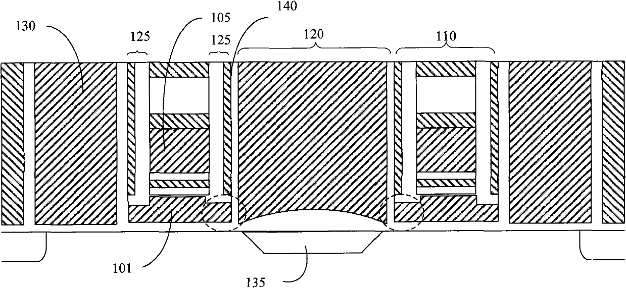
[0039] The method provided by the present invention is not only applicable to discrete gate memory devices, but also to general memory devices with a floating gate structure, especially to memory devices with a feature size of 130nm and below, such as EPROM (Erasable Programmable Read-Only Memo...


PUM


Abstract

The invention relates to a method for forming a discrete gate memory device, which comprises the steps of: providing a semiconductor substrate, wherein a gate dielectric layer, a first polycrystalline silicon layer, an inter-layer insulating layer and a second polycrystalline silicon layer are formed on the semiconductor substrate in sequence, the first polycrystalline silicon layer has a first thickness; etching the second polycrystalline silicon layer and the insulating layer to form a control gate; and etching the first polycrystalline silicon layer to a second thickness, wherein the part of first polycrystalline silicon layer, which is covered by the inter-layer insulating layer, has the first thickness while the part not covered by the inter-layer insulating layer has the second thickness in a range of 80-280. The invention improves the tip shape of a floating gate polycrystal layer by reducing the rest thickness of the floating gate polycrystalline silicon layer by means of smile effect in following technical process and can be suitable for a device in smaller characteristic size and is beneficial to the increase of the erasing speed of the device.

Description

technical field [0001] The invention relates to the field of semiconductor technology, in particular to a method for forming a discrete gate storage device. Background technique [0002] In the current semiconductor industry, integrated circuit products can be mainly divided into three types: analog circuits, digital circuits and digital / analog hybrid circuits, among which storage devices are an important type of digital circuits. Among storage devices, the development of flash memory (flash memory for short) is particularly rapid in recent years. The main feature of flash memory is that it can keep stored information for a long time without power on; and it has the advantages of high integration, fast access speed, easy erasing and rewriting, etc., so it has been widely used in many fields such as microcomputer and automatic control. a wide range of applications. [0003] The standard physical structure of flash memory is called a memory cell (bit). The structure of the ...

Claims


Application Information

Patent Timeline
IPC IPC(8): H01L21/8247H01L21/28H01L27/115H01L29/423
Inventor 李勇刘艳周儒领黄淇生
Owner SEMICON MFG INT (SHANGHAI) CORP
Why Eureka
Try Eureka