Vertical tunneling field effect transistor and its manufacturing method

A tunneling field effect and transistor technology, applied in semiconductor/solid-state device manufacturing, semiconductor devices, electrical components, etc., can solve the problems of small tunneling area and small tunneling current, and increase the tunneling area and tunneling probability. Large, improve the effect of tunneling current

Active Publication Date: 2017-11-17
HUAWEI TECH CO LTD
View PDF4 Cites 0 Cited by
  • Summary
  • Abstract
  • Description
  • Claims
  • Application Information

AI Technical Summary

Problems solved by technology

[0004] At present, tunneling field effect transistors (TFETs) generally adopt vertical tunneling, and vertical tunneling occurs in the source region and channel region under the action of the gate region. Although this method can increase the probability of tunneling, in the prior art, due to The limited overlap area between the source and gate regions results in a smaller tunneling area and thus a smaller tunneling current

Method used


Image

  • Vertical tunneling field effect transistor and its manufacturing method
  • Vertical tunneling field effect transistor and its manufacturing method
  • Vertical tunneling field effect transistor and its manufacturing method

Examples


Embodiment Construction

[0067] The following will clearly and completely describe the technical solutions in the embodiments of the present invention with reference to the accompanying drawings in the embodiments of the present invention. Obviously, the described embodiments are only some, not all, embodiments of the present invention. Based on the embodiments of the present invention, all other embodiments obtained by persons of ordinary skill in the art without creative efforts fall within the protection scope of the present invention.

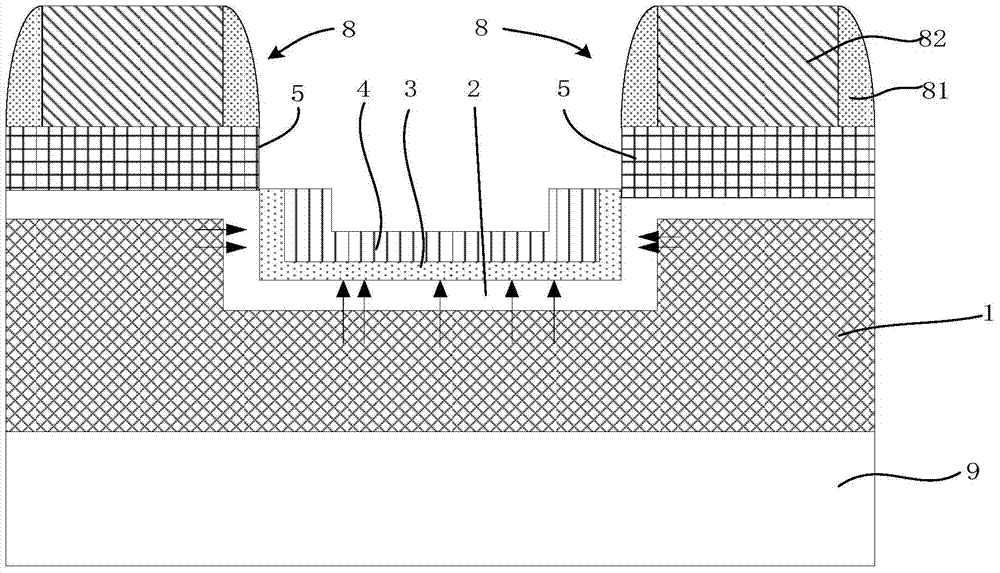
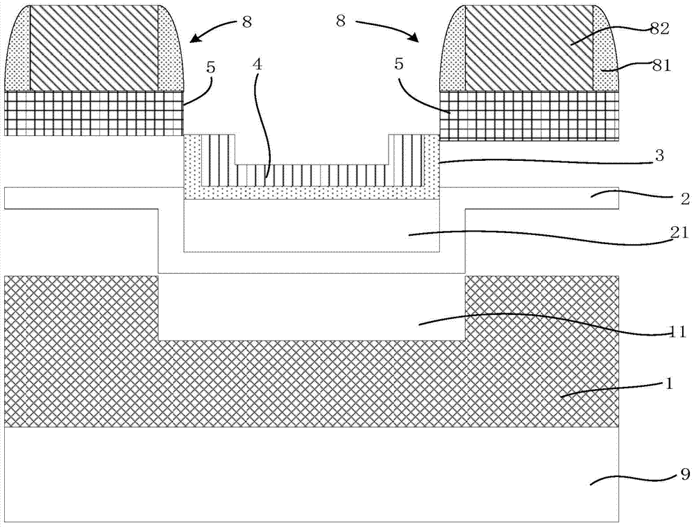
[0068] see figure 1 and figure 2 , is a schematic cross-sectional structure diagram of the vertical tunneling field effect transistor provided in the first preferred embodiment of the present invention. The vertical tunneling field effect transistor includes a source region 1, a first epitaxial layer 2, a gate dielectric layer 3, a gate region 4 and two drain regions 5; the first epitaxial layer 2, the gate dielectric layer 3 and the gate region 4 are sequentiall...


PUM


Abstract

Provided are a vertical tunnelling field-effect transistor and a preparation method therefor. The vertical tunnelling field-effect transistor comprises: a source region (1), a first epitaxial layer (2), a gate dielectric layer (3), a gate region (4) and two drain regions (5). A first groove (11) is provided in the source region. A second groove (21) is provided on the first epitaxial layer, and the first epitaxial layer forms a tunnelling channel between the gate region and the source region. Both the gate dielectric layer and the gate region are provided in the second groove. The two drain regions are respectively provided at two opposite sides outside the second groove. Tunnelling can occur in conduction electrons in an area, overlapped with the gate region, of the first groove of the source region, i.e. an overlapping area between the source region and the gate region is enlarged using the first groove, so that a tunnelling area is enlarged. The first epitaxial layer can form the channel between the gate region and the source region, which involves linear tunnelling, and when the electric field direction of the gate region and the electron tunnelling direction of the source region are on the same line, the tunnelling probability is high, thereby improving a tunnelling current.

Description

technical field [0001] The invention relates to a vertical tunneling field effect transistor and a preparation method thereof. Background technique [0002] Tunneling Field Effect Transistor (TFET) is essentially a gate-controlled reverse-biased PIN diode with different doping types in the source and drain regions. For an N-type tunneling field-effect transistor (TFET), the N-type doping is the drain region, and it is forward biased during operation. P-type doping is the source terminal, and it is negatively biased when working. Compared with metal oxide semiconductor field effect transistors (MOSFETs), tunneling field effect transistors (TFETs) can obtain smaller subthreshold swings (SS), so tunneling field effect transistors (TFETs) are very suitable for low power consume applications. [0003] In a Tunneling Field Effect Transistor (TFET), the process of increasing the output current as the drain voltage increases is through the drain voltage drop at the source tunneli...

Claims


Application Information

Patent Timeline
Patent Type & Authority Patents(China)
IPC IPC(8): H01L29/78H01L21/336
CPCH01L29/78
Inventor 赵静杨喜超张臣雄
Owner HUAWEI TECH CO LTD
Why Eureka
Try Eureka