Germanium tin tunneling field effect transistor and preparation method thereof

A tunneling field effect, transistor technology, applied in semiconductor/solid-state device manufacturing, semiconductor devices, electrical components, etc., can solve the problems of insufficient circuit performance, insufficient driving current, small on-state current, etc., to solve the problem of insufficient driving current, Small forbidden band width, the effect of improving the driving current

Inactive Publication Date: 2015-04-15
PEKING UNIV
View PDF3 Cites 0 Cited by
  • Summary
  • Abstract
  • Description
  • Claims
  • Application Information

AI Technical Summary

Problems solved by technology

However, the on-state current of the silicon tunneling field effect transistor is small, which makes the circuit performance of its application insufficient, so the application is limited
In order to improve the performance of tunneling field effect transistors, many schemes have been proposed, such as using narrow bandgap materials, replacing PIN junctions with PNPN structures, and replacing homojunctions with heterojunction structures. Increase the drive current, but still face the problem of insufficient drive current

Method used


Image

  • Germanium tin tunneling field effect transistor and preparation method thereof
  • Germanium tin tunneling field effect transistor and preparation method thereof
  • Germanium tin tunneling field effect transistor and preparation method thereof

Examples


Embodiment Construction

[0035] The present invention will be further described through the embodiments below in conjunction with the accompanying drawings.

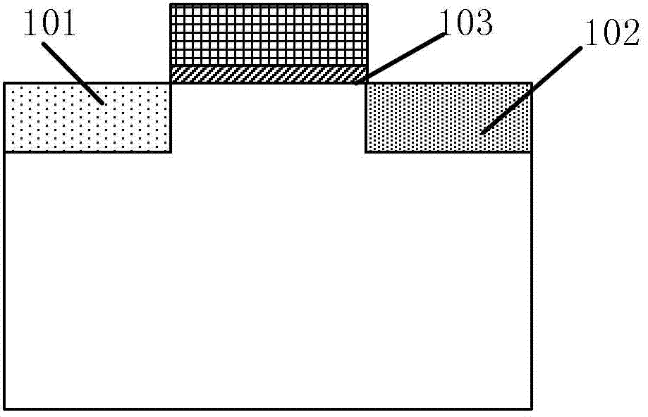
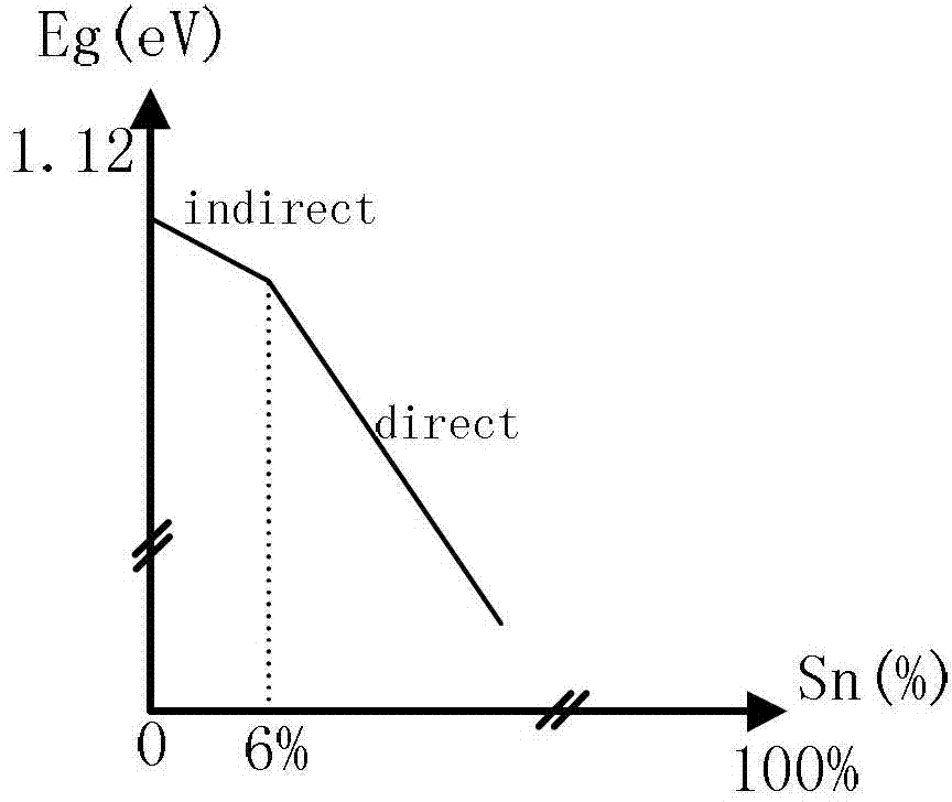
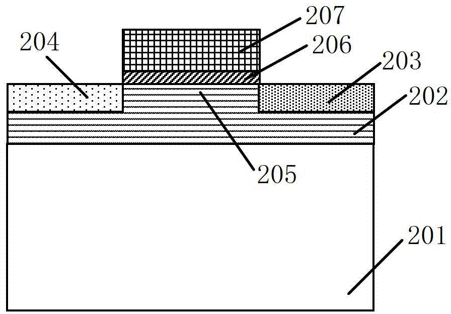
[0036] image 3 is a section of an embodiment of the germanium tin tunneling field effect transistor of the present invention. The germanium-tin tunneling field effect transistor of the present invention comprises a germanium-tin film layer 202, a source region 204, a drain region 203, a channel region 205, a gate stack region and a germanium semiconductor substrate formed on a germanium semiconductor substrate 201 201. Wherein, the gate stack region includes an insulating layer 206 and a conductive layer 207 . The insulating material used for the insulating layer is aluminum oxide, or hafnium oxide, tantalum oxide, and lanthanum oxide high-K gate material; the conductive material for the conductive layer can be aluminum, titanium nitride or tantalum nitride. The source region 204 uses the first doping type, here boron is used; the drain regi...


PUM

PropertyMeasurementUnit
thicknessaaaaaaaaaa

Abstract

The invention discloses a germanium tin tunneling field effect transistor and a preparation method thereof. The germanium tin tunneling field effect transistor comprises a germanium tin film layer, a source region, a drain region, a channel region and a grid stack region which are formed on a substrate of a germanium semiconductor, and the substrate of the germanium semiconductor. The germanium tin tunneling field effect transistor is prepared on the germanium tin film layer growing on the substrate of the germanium semiconductor; the tin content of the germanium tin film layer is regulated in the growing process, and along with increase of the tin content, the forbidden bandwidth of the germanium tin film layer decreases all the time; due to decrease of the forbidden bandwidth of the germanium tin film layer, the tunneling width decreases and the tunneling current obviously increases; and conversion of an indirect band gap into a direct band gap (about 6% of tin) also increases the tunneling current, so that the germanium tin tunneling field effect transistor can increase the driving current significantly, thereby effectively solving the problem of insufficient driving current of the conventional tunneling field effect transistor.

Description

technical field [0001] The invention belongs to semiconductor device technology, and in particular relates to a germanium-tin tunneling field-effect transistor and a preparation method thereof. Background technique [0002] With the continuous shrinking of device size, semiconductor devices are facing many problems, such as serious short channel effect and large leakage current. To address these problems, various solutions have been proposed in the field. Among them, the tunneling field-effect transistor has received extensive attention. It is a new type of low-power device with small subthreshold leakage, subthreshold slope that can break through kT / q, and resistance to short-channel effects. However, the on-state current of the silicon tunneling field effect transistor is small, so that the circuit performance of the silicon tunneling field effect transistor is insufficient, so the application is limited. In order to improve the performance of tunneling field effect tran...

Claims


Application Information

Patent Timeline
Patent Type & Authority Patents(China)
IPC IPC(8): H01L29/36H01L29/739H01L21/331
Inventor 黄如邱颖鑫
Owner PEKING UNIV
Why Eureka
Try Eureka