

Light-emitting device
A technology of light-emitting devices and light-emitting chips, applied in the direction of lighting devices, light sources, components of lighting devices, etc., can solve problems such as unevenness, increased manufacturing costs, changes, etc., achieve high-efficiency light output, prolong service life, and avoid light Fading effect
- Summary
- Abstract
- Description
- Claims
- Application Information
AI Technical Summary
Problems solved by technology
Method used
Image

Examples
no. 1 example
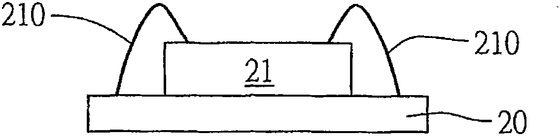
[0040] The present invention relates to the technology of LED light source, and the photonic crystal technology cooperates with the existing packaging technology; please refer to Figures 2A to 2D , is the manufacturing method of the first embodiment of a light-emitting device provided by the present invention.
[0041] Such as Figure 2A As shown, at least one light-emitting chip 21 is arranged on a substrate 20; the substrate 20 is, for example, a circuit board, a lead frame or a reflective cup, etc., and there is no specific limitation. In this embodiment, a circuit board is used for illustration; The light emitting chip 21 mentioned above is a light emitting diode (light emitting diode, LED). , is a well-known technology in the industry, and is not limited to the above-mentioned wire-bonding method, and it is not a technical feature of this case, so it will not be described in detail, and is hereby stated.
[0042] Such as Figure 2B As shown, an encapsulation layer 22 of...
no. 2 example
[0054] see Figures 3A to 3D , discloses the manufacturing method of the second embodiment of the light-emitting device of the present invention. The difference between this embodiment and the first embodiment lies only in the formation position of the optical crystal layer, and the designs of other related light-emitting devices are roughly the same, so the structure and function of the same parts will not be described repeatedly, and only the differences will be described below. It is hereby stated.
[0055] Such as Figure 3A As shown, at least one light-emitting chip 31 is disposed on a substrate 30 .
[0056] Such as Figure 3B As shown, an optical crystal layer 33 is formed on the surface of the light-emitting chip 31, and the optical crystal layer 33 is a structure composed of a multi-nanoparticle arrangement, as shown in the figure. Formed on the light-emitting wafer 31 by means of electron beam lithography or electron beam lithography.
[0057] Such as Figure 3...
PUM
 Abstract
Description
Claims
Application Information