Non-CMP preparation technology applicable to back grid technology

A technology of preparation process and gate-last process, which is applied in the field of planarization preparation process suitable for gate-last process without CMP, can solve the problems of difficult control, high cost of CMP planarization process, expensive equipment, etc., and achieve the effect of low cost

Active Publication Date: 2011-05-11
BEIJING YANDONG MICROELECTRONICS
View PDF0 Cites 6 Cited by
  • Summary
  • Abstract
  • Description
  • Claims
  • Application Information

AI Technical Summary

Problems solved by technology

[0003] In order to overcome the shortcomings of high cost, expensive equipment and difficult control of the CMP planarization process in the gate-last process, the present invention provides a low-cost planarization process without a CMP process, which is simple in process and easy to monitor, and is comparable to the CMOS process Good compatibility, which facilitates the integration of replacement gates in the gate-last process

Method used


Image

  • Non-CMP preparation technology applicable to back grid technology

Examples


Embodiment Construction

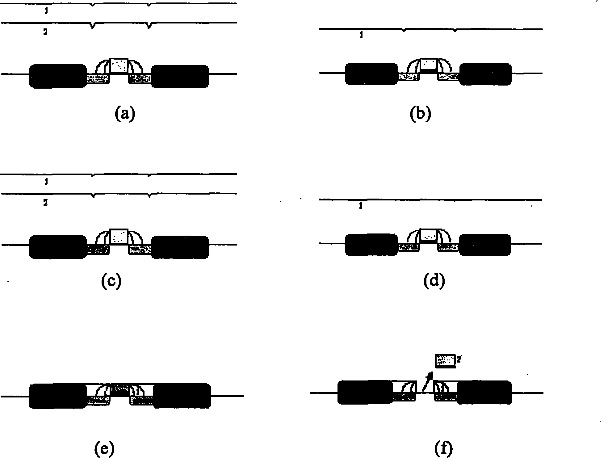
[0024] see figure 1 , the planarization process flow of the present invention is as follows:

[0025] It should be noted that figure 1 middle:

[0026] (a) Spin-coating primary photoresist: 1 is primary photoresist; 2 is dielectric (LTO+Si 3 N 4 );

[0027] (b) After one photoresist back-etching, photoresist / LTO rate difference back-etching and deglue: 1 is the remaining medium (LTO+Si 3 N 4 );

[0028] (c) Spin-coating secondary photoresist: 1 is the secondary photoresist, 2 is the remaining medium (LTO+Si 3 N 4 );

[0029] (d) After two times of photoresist back etching, photoresist / LTO equal speed back etching and deglue: 1 is the remaining medium (LTO+Si 3 N 4 );

[0030] (e) Etch LTO to expose the dummy gate: 1 is the remaining dielectric (LTO+Si 3 N 4 );

[0031] (f) Remove the dummy gate: 1 is the remaining dielectric (LTO+Si 3 N 4 ), 2 is a false gate.

[0032] The above process flow is the main steps of the present invention, on the basis of which, t...


PUM


Abstract

A non-CMP (chemical mechanical planarization) preparation technology applicable to back grid technology comprises the following steps: utilizing photoresist which is generally adopted in CMOS (Complementary Metal Oxide Semiconductor) technology and has favorable fluidity after dilution to fill the valley of rough patterns, to ensure that the surface of the pattern is basically flat after glue is spin-coated; taking the photoresist as a carrier, removing LTO (low-temperature oxide) on the raised pattern through utilizing speed difference recording method of the photoresist and the LTO, and an approximately flat surface is obtained since the active zone of a device is protected against erosion by residual glue; performing glue coating again to record the photoresist and the LTO in the same speed rate to realize full-planarization; and recording medium to the exposed end of a false gate electrode to remove the polycrystalline silicon false gate electrode and deposit needed metal grid thin film. The preparation technology has the advantages that special equipment is not needed to be additionally arranged, the technology and the monitoring are simple, the compatibility with the CMOS technology is better, and convenience is brought for the integration of replace grid in the back grid technology.

Description

technical field [0001] The invention belongs to a nanoscale semiconductor device preparation process, relates to a non-CMP planarization process technology, and is a necessary means for preparing a nanoscale gate-last process CMOS (complementary metal oxide semiconductor) device. technical background [0002] The current development of integrated circuits has entered the technology generation of 45nm node and below. In order to reduce the serious gate tunneling leakage current of ultra-thin gate dielectric and eliminate the depletion effect of polysilicon gate, high dielectric constant (K) gate dielectric / metal gate electrode is adopted. It is imperative to replace the traditional SiON gate dielectric / polysilicon gate electrode structure with an integrated structure. The high-K gate dielectric / metal gate structure is divided into gate-first process and gate-last process. Since the gate-last process is an integrated process of gate process after the source and drain are forme...

Claims


Application Information

Patent Timeline
Patent Type & Authority Applications(China)
IPC IPC(8): H01L21/336H01L21/28
Inventor 徐秋霞钟兴华
Owner BEIJING YANDONG MICROELECTRONICS
Why Eureka
Try Eureka