
Contact image sensing chip and module

An image sensing and contact technology, applied in image communication, electrical components, etc., can solve the problem that the human eye cannot detect the small misalignment of the image

Inactive Publication Date: 2011-05-11
CREATIVE SENSOR INC
View PDF0 Cites 0 Cited by
  • Summary
  • Abstract
  • Description
  • Claims
  • Application Information

AI Technical Summary

Problems solved by technology

[0011] refer to Figure 2b , when the image sensing pixels 120 of two adjacent image sensing chips 10 have a slight gap d1 in the Y-axis direction, but still have a partial overlapping area, assuming that the scanned image is a straight line, the read to the image as Figure 3b As shown, although the two line segments 51 and 52 are slightly misaligned, they are still connected at least. Since the actual size of the image is extremely small, the human eye cannot detect the slight misalignment of the image

Method used


Image

  • Contact image sensing chip and module
  • Contact image sensing chip and module
  • Contact image sensing chip and module

Examples


Embodiment Construction

[0042] Below in conjunction with accompanying drawing, structural principle and working principle of the present invention are specifically described:

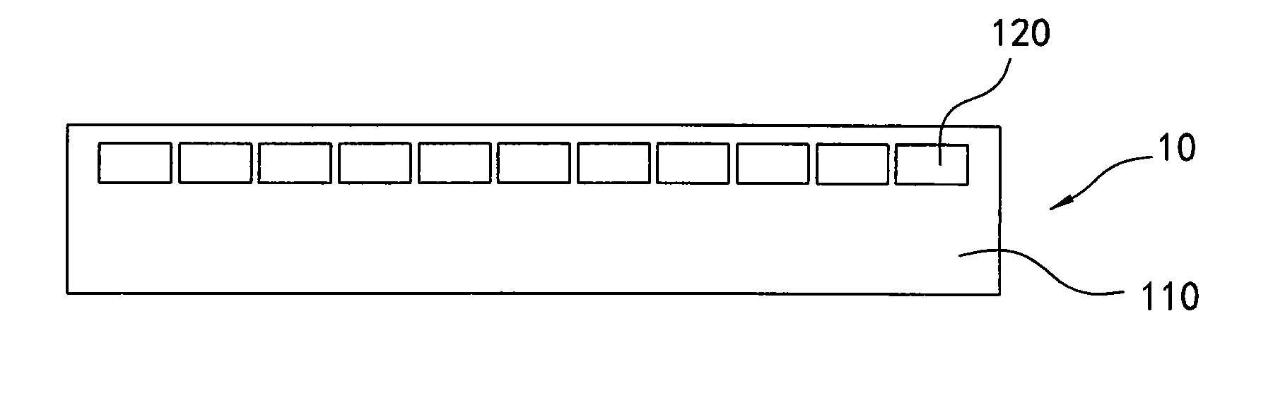
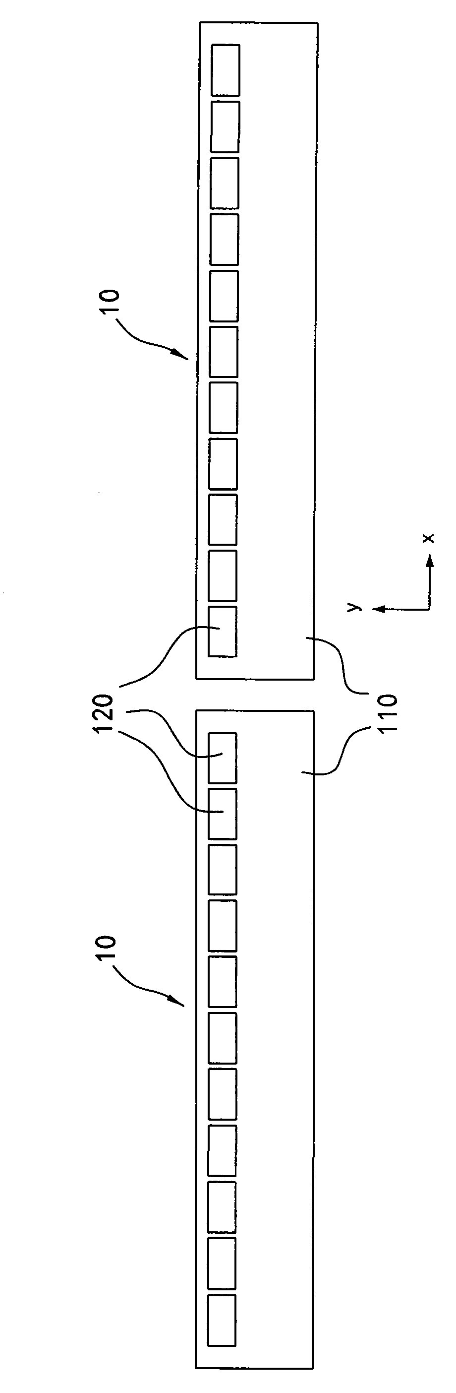
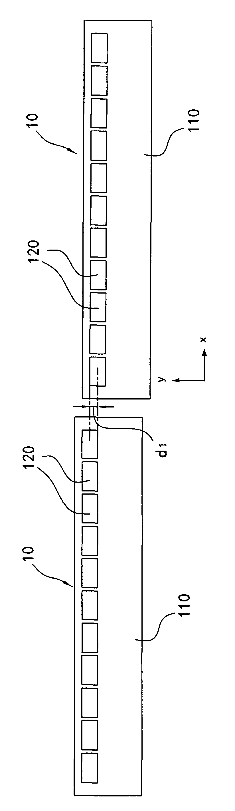
[0043] Cooperate with reference Figure 4, is a schematic diagram of the appearance of the image sensing chip 20 of the present invention. The image sensing chip 20 includes a substrate 210 and a plurality of image sensing pixels 220 . The image sensing pixels 220 are disposed on the substrate 210 extending along an X-axis direction, and there is an equidistant gap between each of the image sensing pixels 220 . Wherein each of the image sensing pixels 220 has the same length along the X-axis direction, and the length of each of the image sensing pixels 220 along a Y-axis direction perpendicular to the X-axis direction varies with the position placed on the substrate 210 However, the length of the image sensing pixels 220 located in the middle of the substrate 210 along the Y-axis direction is shorter, and the length of the i...


PUM


Abstract

The invention provides a contact image sensing chip, which is arranged inside a contact image sensing module. The contact image sensing module comprises a plurality of contact image sensing chips; the contact image sensing chips are arranged in a row along an X axis in an extending manner so as to correspondingly capture a transverse row of images; each of the contact image sensing chips comprises a substrate and a plurality of image sensing pixels; these image sensing pixels are arranged on the substrate along the X-axis direction in the extending manner; an equidistant gap is reserved between every two of the sensing pixels, wherein the length of each of the image sensing pixels along the X-axis direction is equal to the length of the image sensing pixel positioned in the middle of the corresponding image sensing chip along a Y-axis direction vertical to the X-axis direction; and the lengths of the image sensing pixels adjacent to the edge of the substrate are increased along the Y-axis direction.

Description

technical field [0001] The invention relates to an image sensing chip, in particular to an image sensing chip used in a contact image device. Background technique [0002] Contact Image Sensor (Contact Image Sensor, CIS) is a kind of linear image sensor, which is used to scan flat images or documents into electronic format for storage, display or transmission. Its main applications are scanners, fax Machines and multi-function business machines. [0003] The working principle of the contact image sensor is to irradiate the light generated by a light source onto the manuscript to be scanned, reflect the light through the manuscript, and use a lens group to gather the reflected light to the Charge-Coupled Device (CCD) Or on a photosensitive component such as a Complementary Metal Oxide Semiconductor (CMOS), the photosensitive component is used to change the light signal into an electrical signal, and then generate analog or digital pixel (pixel) data. During the scanning pro...

Claims


Application Information

Patent Timeline
IPC IPC(8): H04N1/028H04N1/031
Inventor 陈鸿吉李政贾礼卫
Owner CREATIVE SENSOR INC
Learn More