Ball grid array (BGA) package structure

A ball grid array and structure technology, which is applied in semiconductor/solid-state device components, semiconductor devices, electrical components, etc., can solve problems such as unfavorable wire material costs, punching defects, and reducing the overall package length, width, and height.

Inactive Publication Date: 2011-05-25
ASE ASSEMBLY & TEST SHANGHAI
View PDF4 Cites 6 Cited by
  • Summary
  • Abstract
  • Description
  • Claims
  • Application Information

AI Technical Summary

Problems solved by technology

[0005] However, the BGA packaging structure still has the following problems in the actual wire bonding and molding process, for example: when the wire bonding, when the length of the first wire 13 and/or the second wire 14 is too long Or when the arrangement is too dense, the adjacent upper and lower layer wires are likely to accidentally contact each other due to defects such as line collapse, which will cause short circuit problems
Even if no contact short circuit is caused during wiring, it is still easy to cause punching defects of adjacent left and right wires (or upper and lower layer wires) due to the flow impact force of the encapsulant 16 during the subsequent molding process and contact short circuit

Method used


Image

  • Ball grid array (BGA) package structure
  • Ball grid array (BGA) package structure
  • Ball grid array (BGA) package structure

Examples


Embodiment Construction

[0030] The following descriptions of the various embodiments refer to the accompanying drawings to illustrate specific embodiments in which the invention may be practiced. Furthermore, the directional terms mentioned in the present invention, such as "up", "down", "front", "rear", "left", "right", "inside", "outside" or "side", etc., Only refer to the directions of the attached drawings. Therefore, the directional terms used are for describing and understanding the present invention, not for limiting the present invention.

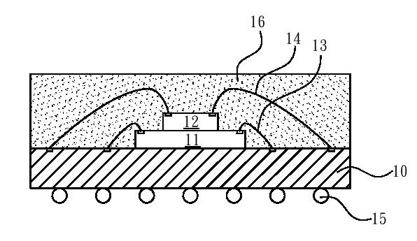
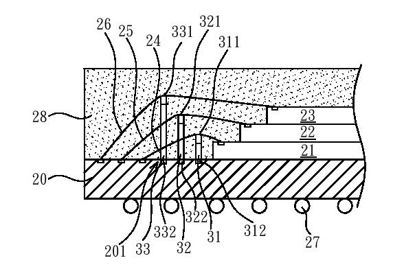
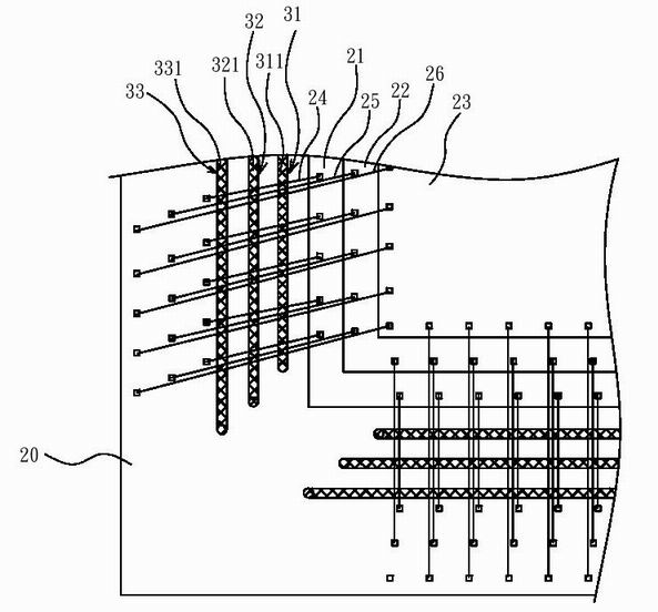
[0031] The present invention is mainly applied to a ball grid array (BGA) package structure with stacked dies, wherein the BGA package structure preferably has three or more chips and three or more layers of wires; the ball grid The length and width dimensions of the array package structure are preferably equal to or greater than 21×21 mm (millimeters); and the total number of wires on each side of the ball grid array package structure is preferably equal...


PUM

PropertyMeasurementUnit
Wire diameteraaaaaaaaaa

Abstract

The invention discloses a ball grid array (BGA) package structure, which is characterized in that wire carriages are utilized to support corresponding wires so as to prevent the wires from collapsing in a vertical direction, and effectively separate the wires in an upper layer from the wires in a lower layer. Meanwhile, the wire carriages are provided with rough insulating surfaces, and can further prevent the wires from deviating and being rushed in a horizontal direction. Therefore, the structure can effectively avoid the wires in any two adjacent layers or the left and right wires from generating contact short circuit.

Description

technical field [0001] The present invention relates to a ball grid array packaging structure, in particular to a ball grid array packaging structure that utilizes a wire support frame to effectively avoid contact short-circuiting of adjacent wires. Background technique [0002] Nowadays, in order to meet the needs of various high-density packaging, the semiconductor packaging industry has gradually developed various types of packaging designs, among which various system in package (SIP) design concepts are often used to construct high-density packaging products. Generally speaking, system-in-package can be classified into a multi-chip module (MCM), a package on package (POP), a package in package (PIP), and the like. The multi-chip module (MCM) refers to the arrangement of several chips on the same substrate. After the chips are arranged, the same packaging colloid is used to embed all the chips, and they can be subdivided into stacked chips according to the arrangement of ...

Claims


Application Information

Patent Timeline
IPC IPC(8): H01L23/31H01L23/498H01L25/065
CPCH01L2224/48997H01L2924/15311H01L2924/10253H01L24/48H01L2224/48227H01L2924/181H01L2224/05554H01L2224/48H01L2924/00H01L2924/00012
Inventor 于睿
Owner ASE ASSEMBLY & TEST SHANGHAI
Why Eureka
Try Eureka