Groove metal-oxide semiconductor field effect transistor and manufacture method thereof

An oxide semiconductor and field effect transistor technology, which is applied in semiconductor/solid-state device manufacturing, semiconductor devices, transistors, etc., can solve problems such as large leakage current, achieve high breakdown voltage, low gate leakage charge, and save production costs. Effect

Active Publication Date: 2011-05-25
FORCE MOS TECH CO LTD
View PDF2 Cites 18 Cited by
  • Summary
  • Abstract
  • Description
  • Claims
  • Application Information

AI Technical Summary

Problems solved by technology

This structure will cause a large leakage current between the drain and source, because under the drain/source bias voltage, the P-type body regio

Method used


Image

  • Groove metal-oxide semiconductor field effect transistor and manufacture method thereof
  • Groove metal-oxide semiconductor field effect transistor and manufacture method thereof
  • Groove metal-oxide semiconductor field effect transistor and manufacture method thereof

Examples


Example Embodiment

[0068] The present invention will be described in detail below with reference to the drawings, in which preferred embodiments of the present invention are shown. The present invention can, but be embodied in different ways, but should not be limited to the embodiments described herein. For example, the description here refers more to N-channel trench MOSFETs, but it is obvious that other devices are also possible.

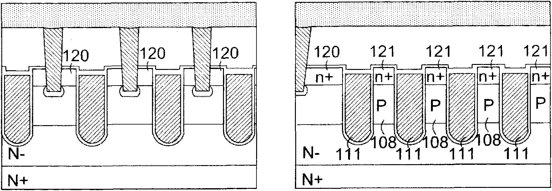
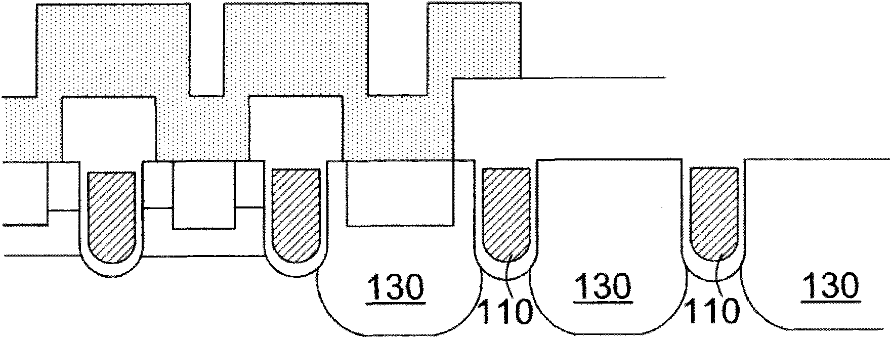
[0069] Reference image 3 As shown in a preferred embodiment of the present invention, the N-type epitaxial layer 202 is formed on the N+ substrate 200, and a drain metal 290 is deposited on the lower surface of the N+ substrate 200. In the N-type epitaxial layer 202, there are a plurality of first trench gates 210 located in the active area, at least one wider second trench gate 212 for gate connection, and at least three second trench gates located in the terminal area. Three trench gate 211. The inner surfaces of the first trench gate 210, the second trench gate ...


PUM


Abstract

The invention discloses a grooved metal-oxide semiconductor field effect transistor and a manufacture method thereof. The depth of terminal area groove gratings is more than or equal to the junction depth of a terminal area midbody zone, and the zone between every two adjacent terminal area groove gratings also has a suspended voltage, therefore, an element has higher breakdown voltage and lower gate-drain charge.

Description

Technical field [0001] The invention relates to a unit structure, device structure and process manufacturing of a semiconductor power device, in particular to a unit structure and process method of a trench MOSFET (metal oxide semiconductor field effect transistor). Background technique [0002] In the prior art, the traditional trench metal oxide semiconductor field effect transistor (MOSFET) structure that uses a trench gate with a floating voltage as a terminal region is encountering severe technical challenges. For example, in the prior art of U.S. Patent No. 6,462,376, a trench MOSFET structure using a trench gate with a floating voltage as the terminal region is disclosed. At the same time, the n+ source region 121 is located in every two adjacent terminal regions. Between the trench gates 111, such as Figure 1A Shown. This structure will cause a large leakage current between the drain and the source, because under the drain / source bias voltage, the P-type body region 108 ...

Claims


Application Information

Patent Timeline
IPC IPC(8): H01L27/088H01L29/78H01L29/423H01L21/8234H01L21/336H01L21/28
Inventor 谢福渊
Owner FORCE MOS TECH CO LTD
Why Eureka
Try Eureka