Integrated circuit structure
A technology of integrated circuits and dielectric materials, which is applied in the field of semiconductor fins and fin field effect transistors and their formation, and can solve problems such as affecting the performance of integrated circuits.
- Summary
- Abstract
- Description
- Claims
- Application Information
AI Technical Summary
Problems solved by technology
Method used
Image

Examples
Embodiment Construction
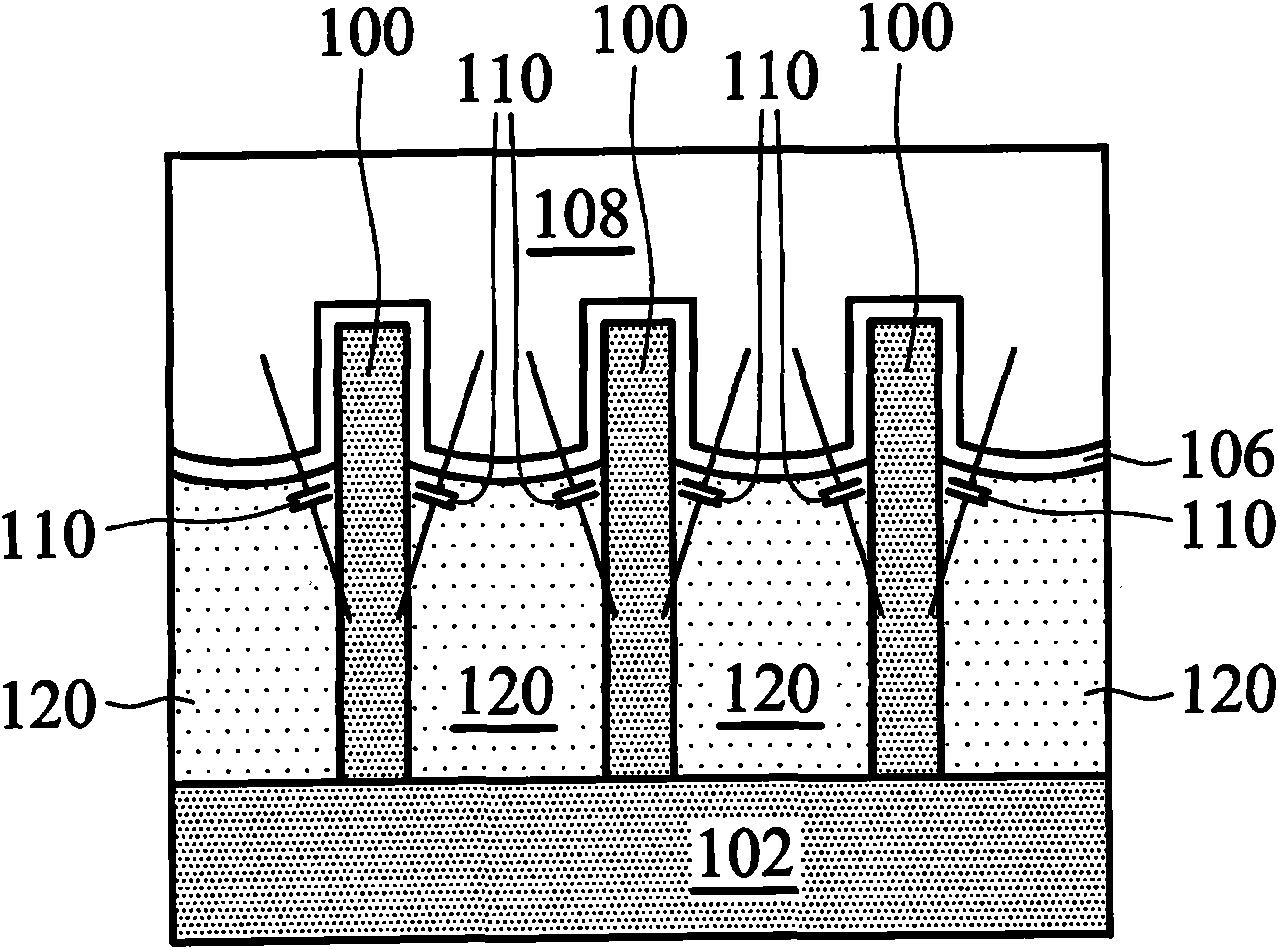
[0053] Novel methods of forming Fin field-effect transistors (FinFETs) are provided. Intermediate stages in the manufacture of an embodiment are illustrated. Variations of embodiments are discussed. The same reference numerals are used to represent the same elements throughout the different drawings and illustrated embodiments.
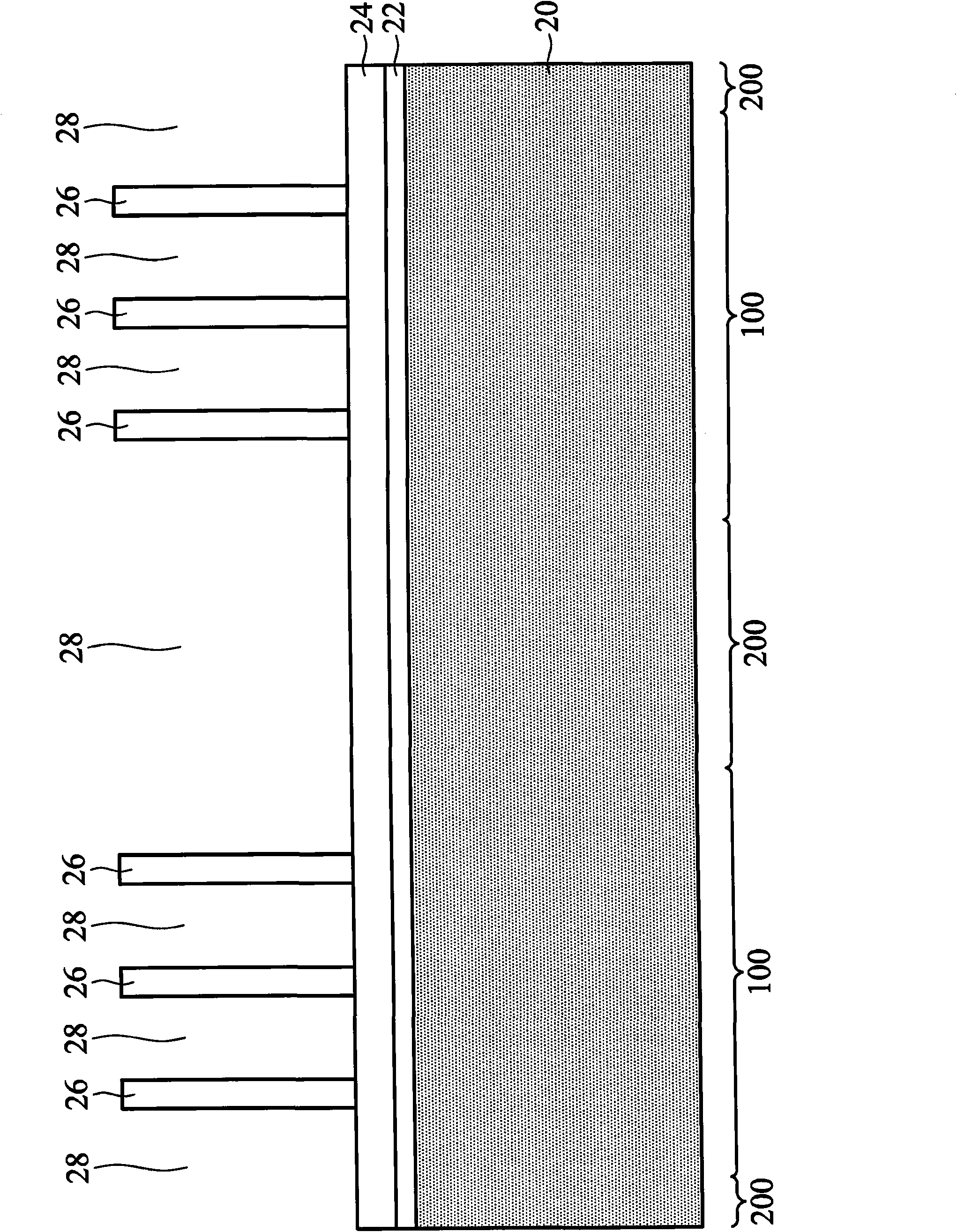
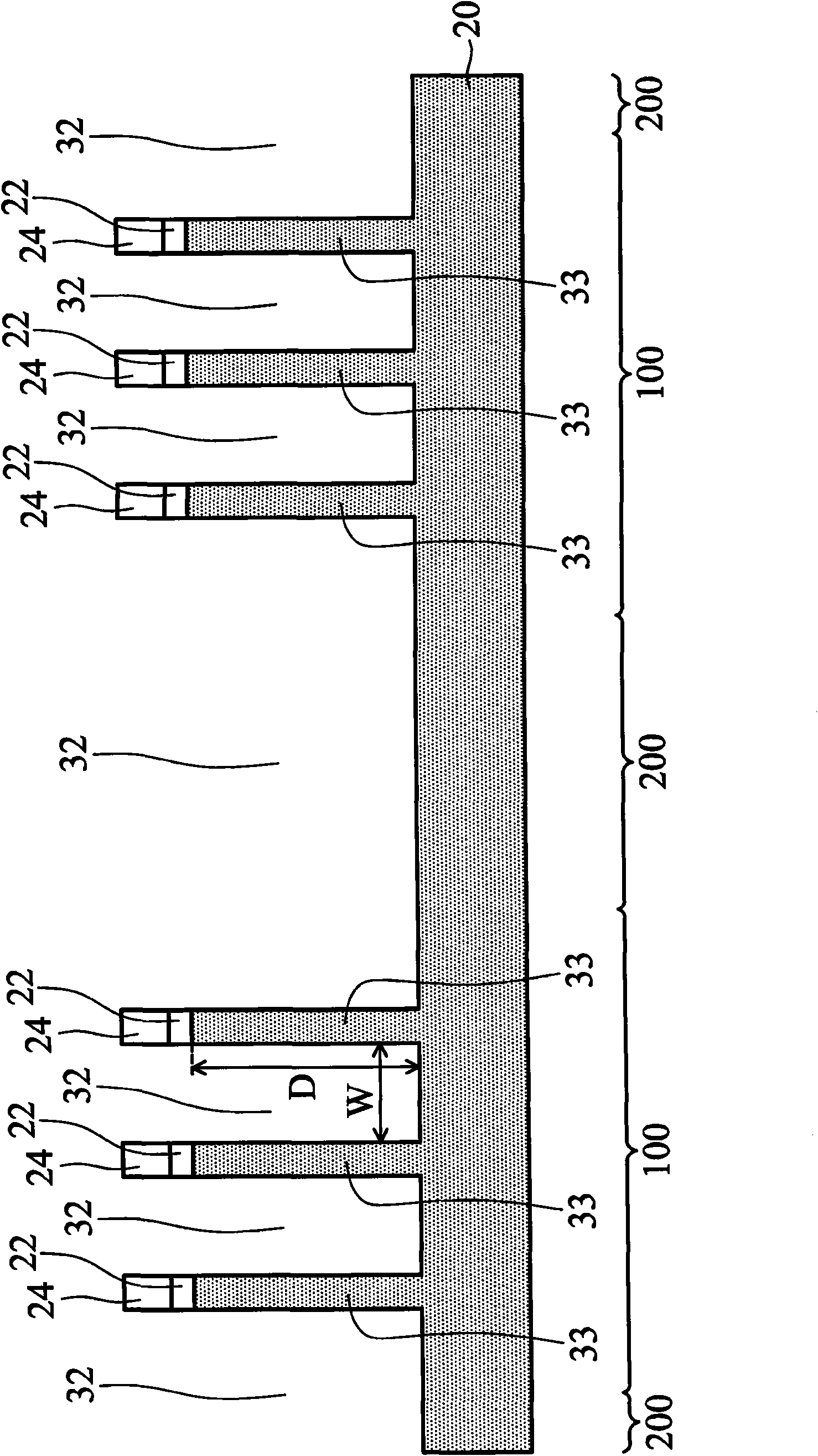
[0054] see figure 2 , providing a semiconductor substrate 20 . In one embodiment, the semiconductor substrate 20 includes silicon. Other commonly used materials such as carbon, germanium, gallium, arsenic, nitrogen, indium, and / or phosphorus, and the like may also be included in the semiconductor substrate 20 . The semiconductor substrate 20 can be a bulk substrate or a semiconductor-on-insulator substrate. The semiconductor substrate 20 includes a portion in an intra-device region 100 and a portion in an inter-device region 200 . Each inner device region 100 may be used to form a FinFET, and the inner device regions 100 may be separated from e...
PUM
 Abstract
Description
Claims
Application Information
 - R&D
- Intellectual Property
- Life Sciences
- Materials
- Tech Scout
- Unparalleled Data Quality
- Higher Quality Content
- 60% Fewer Hallucinations
Browse by: Latest US Patents, China's latest patents, Technical Efficacy Thesaurus, Application Domain, Technology Topic, Popular Technical Reports.
© 2025 PatSnap. All rights reserved.Legal|Privacy policy|Modern Slavery Act Transparency Statement|Sitemap|About US| Contact US: help@patsnap.com