A double silicon nanowire wrap gate field-effect transistor and its manufacture method

A technology of field-effect transistors and silicon nanowires, which is applied in semiconductor/solid-state device manufacturing, semiconductor devices, electrical components, etc., can solve the problems of reducing device switching speed, increasing gate capacitance, and increasing leakage current, so as to improve the performance of devices. Effects of switching speed, reduction of parasitic gate capacitance, and reduction of leakage current

Inactive Publication Date: 2007-10-24
PEKING UNIV
View PDF0 Cites 28 Cited by
  • Summary
  • Abstract
  • Description
  • Claims
  • Application Information

AI Technical Summary

Problems solved by technology

[0003] However, the silicon nanowire multi-gate or surrounding gate devices that have been reported are either limited by the structure itself, or will bring difficulties in process preparation, etc., so that the advantages of silicon nanowire multi-gate or surrounding gate devices are often not fully reflected.
[0004] For example, the nanowire Ω gate device shown in Document 1 (F.L.Yang, D.H.Lee, H.Y. Chen, et al., "5nm-gate nanowire FinFET", in Symp.VLSl Tech.Dig, 2004, pp:196-197) (As shown in Figure 2(a)-(d)), there are the following problems: (1) it is prepared on an SOI substrate, and the cost is very high; (2) because the preparation of silicon nanowires requires a very thin top silicon film, SOI The channel on the substrate has the same thickness as the silicon film of the source and drain, as shown in Figure 2(c), which increases the parasitic series resistance of the source and drain and limits the on-state drive current; (3) at the same time, the silicon nanowire device The cross-sectional structure along the vertical direction of the channel is an Ω gate structure, as shown in Figure 2(b) and (d), which is not a surrounding gate structure, and the gate control capability needs to be further improved
[0006] However, there is still a very serious problem in the device with this structure: as shown in Figure 3 (b) and (c), there is a parasitic tube on the surface of the bulk silicon substrate directly below the double silicon nanowire, which is formed by Parasitic gate oxide, parasitic channel and shared source, drain and polysilicon gate composition
Therefore, the device with this structure shown in Document 2 has the following disadvantages: (1) The parasitic tube increases the leakage current of the entire device and reduces the switching ratio, which increases the power consumption of the device and is not suitable for low-power logic ( Low-power Logic) applications; (2) The gate capacitance of the parasitic tube also increases the total gate capacitance, which deteriorates the AC characteristics of the device and reduces the switching speed of the device, which is not suitable for high-speed logic (High-speed Logic) applications; (3) At the same time, in the process preparation, the SiGe corrosion sacrificial layer in Document 2 and the silicon channel as the nanowire are all grown epitaxially, and the process cost is still very high

Method used


Image

  • A double silicon nanowire wrap gate field-effect transistor and its manufacture method
  • A double silicon nanowire wrap gate field-effect transistor and its manufacture method
  • A double silicon nanowire wrap gate field-effect transistor and its manufacture method

Examples


Embodiment Construction

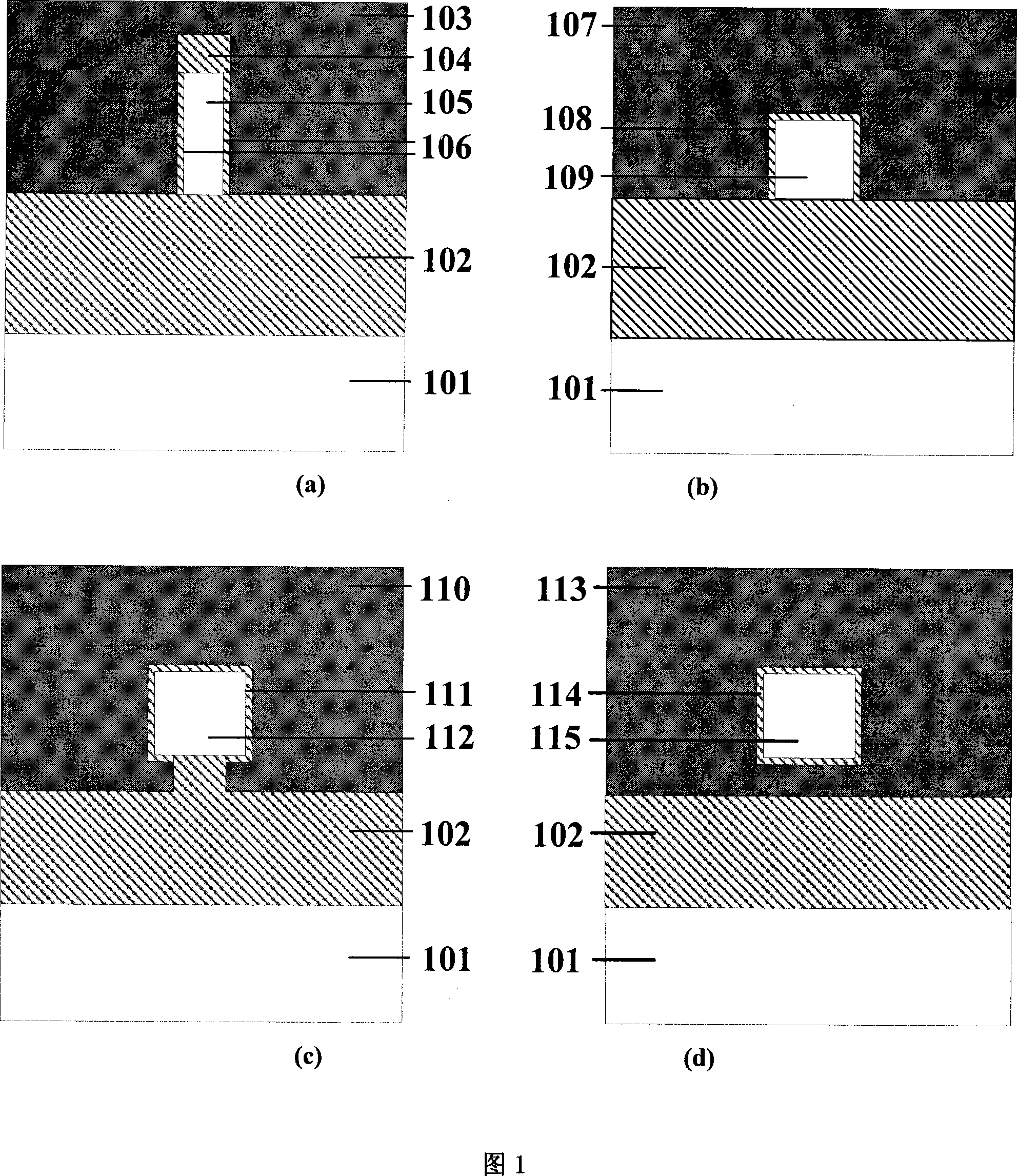
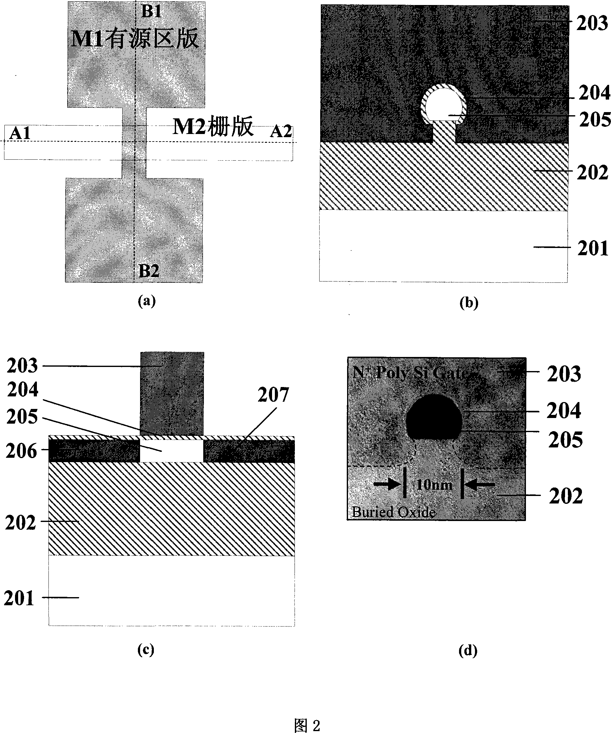
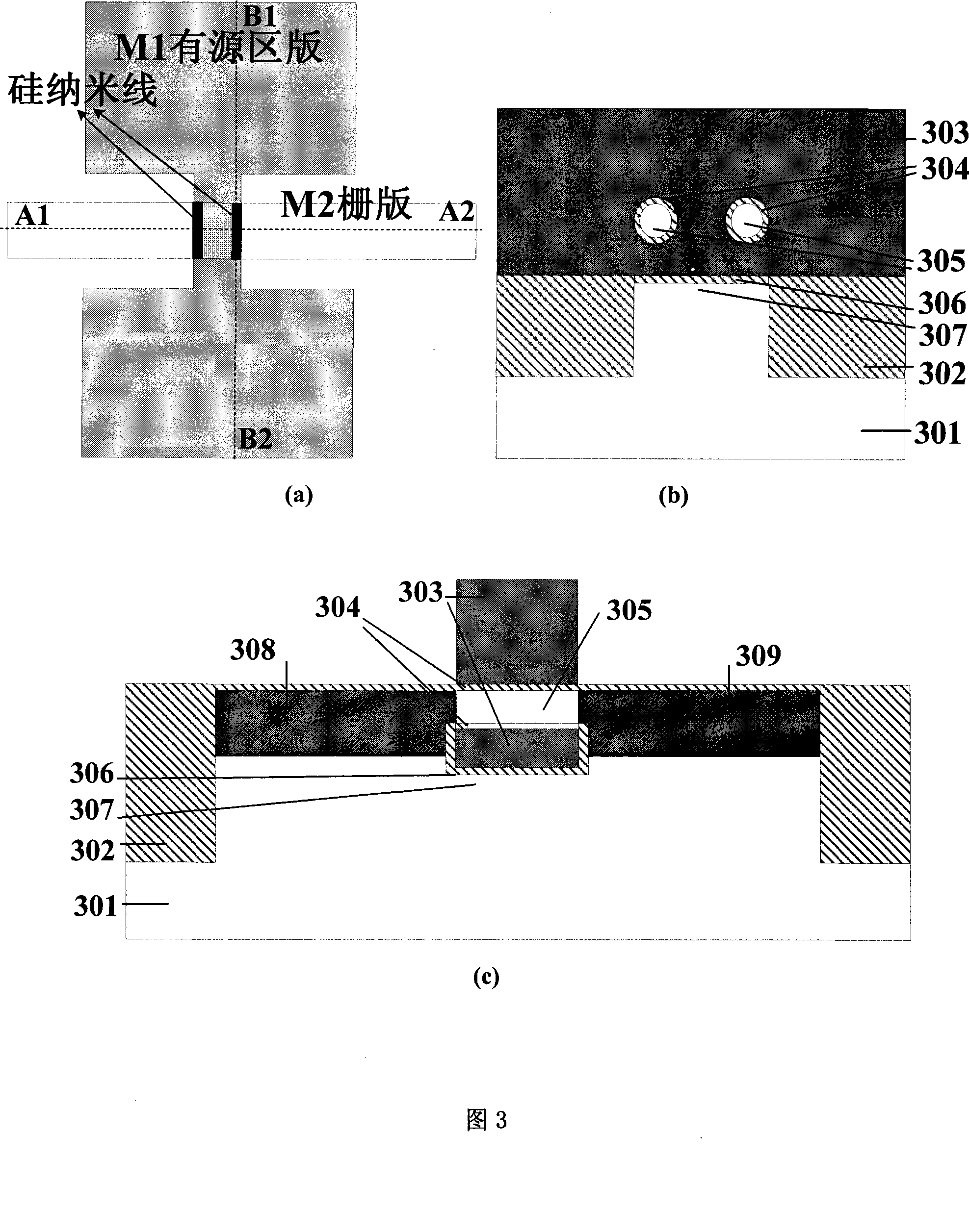
[0074] The double silicon nanowire gate field effect transistor provided by the present invention and its preparation method will be described in detail below with reference to the accompanying drawings, but this does not constitute a limitation to the present invention.

[0075] As shown in FIG. 4 , it is the double silicon nanowire gate device of this embodiment. Figure 4(a) shows the layout of the device. The part of the M1 active region plate covered by the M2 gate plate is the channel region, and the uncovered part is the source region and drain region. The width of the channel region (A1A2 direction) is 50nm, and the length of the channel region (B1B2 direction), that is, the gate length is 30nm. Figure 4(b) and (c) respectively show the cross-sectional structure of the device along the vertical direction of the channel (A1A2 direction) and along the channel direction (B1B2 direction). As shown in Figure 4(b): the cross section of the double silicon nanowire 405 as a ch...


PUM


Abstract

The provided double-silicon nano line enclose-grid FET belonged to MOSFET technique in ULSI comprises: a silicon substrate, double silicon lines as the channels, a grid anode and multicrystal silicon grid enclosing the nano lines to form the enclose-grid structure, both source and drain connecting with the substrate, and a thick SiO2 layer between the right bottom of channel and substrate. This invention is compatible to common CMOS technique, reduces cost and power consumption, and has wide application.

Description

technical field [0001] The invention belongs to the technical field of metal oxide semiconductor field effect transistor (MetalOxide Silicon Field Effect Transistor-MOSFET) in ultra-large scale integrated circuit (ULSI), in particular to a field effect transistor surrounded by double silicon nanowires and a preparation method thereof. Background technique [0002] With the wide application and high-speed development of VLSI, MOSFET technology has entered the nanometer field (<100nm). However, when the gate length of a conventional single-gate MOSFET (which can be referred to as a device) is scaled down to sub-50nm, problems such as poor gate control capability, deterioration of short-channel effect, large leakage current, and insufficient on-state drive current will become more apparent. It's getting serious. In order to improve the gate control ability of MOSFET as much as possible, reduce the leakage current, increase the on-state drive current, increase the switching ...

Claims


Application Information

Patent Timeline
Patent Type & Authority Applications(China)
IPC IPC(8): H01L29/78H01L21/336
Inventor 周发龙吴大可黄如诸葛菁田豫张兴
Owner PEKING UNIV
Why Eureka
Try Eureka