Isolating method for silicon mesa vertical channel field effect transistor
A technology of transistors and dojos, applied in semiconductor/solid-state device manufacturing, electrical components, circuits, etc., to achieve the effect of reducing parasitic gate capacitance, broad application prospects, and optimizing DC and AC characteristics
- Summary
- Abstract
- Description
- Claims
- Application Information
AI Technical Summary
Problems solved by technology
Method used
Image

Examples
Embodiment Construction
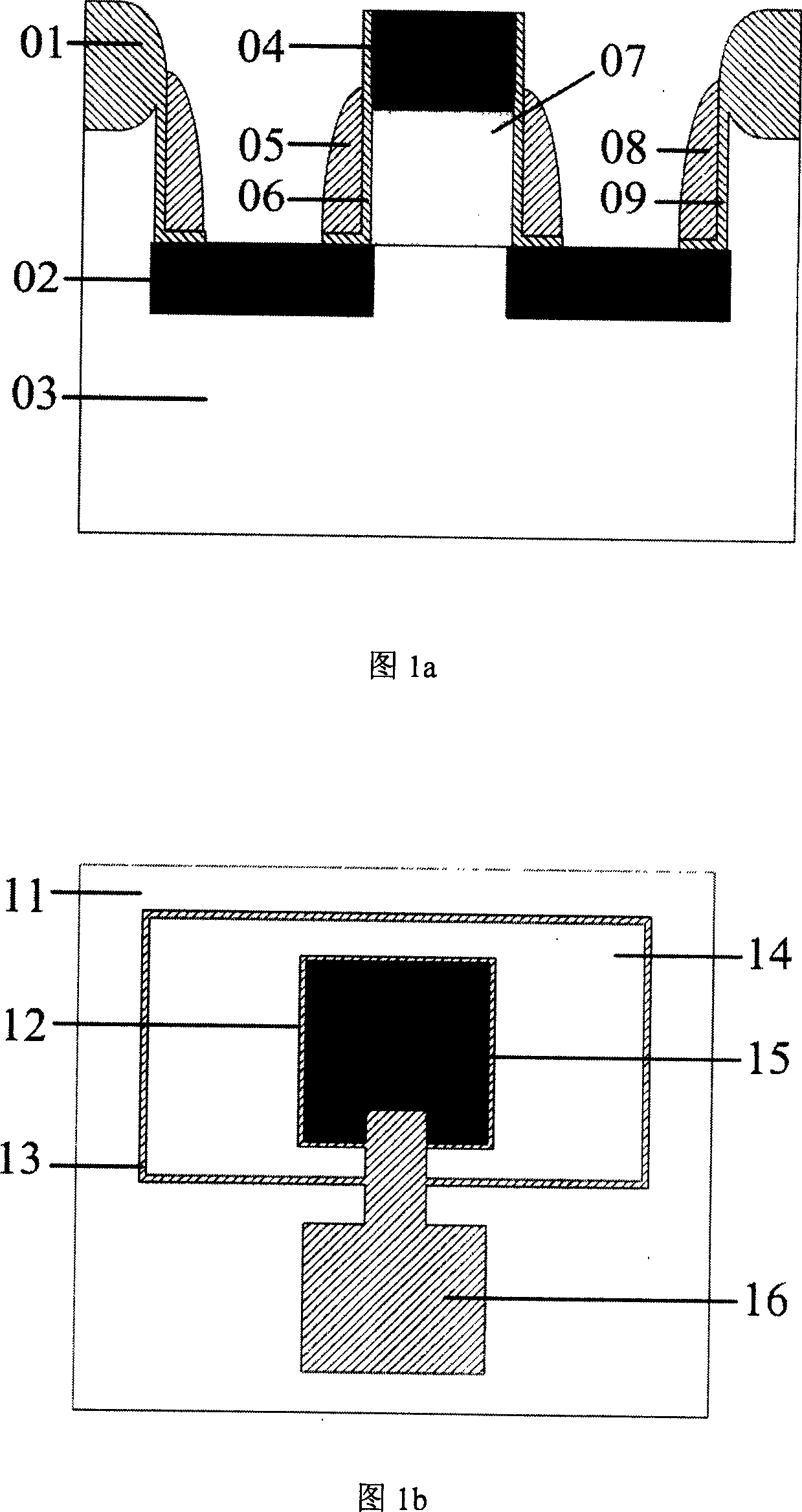
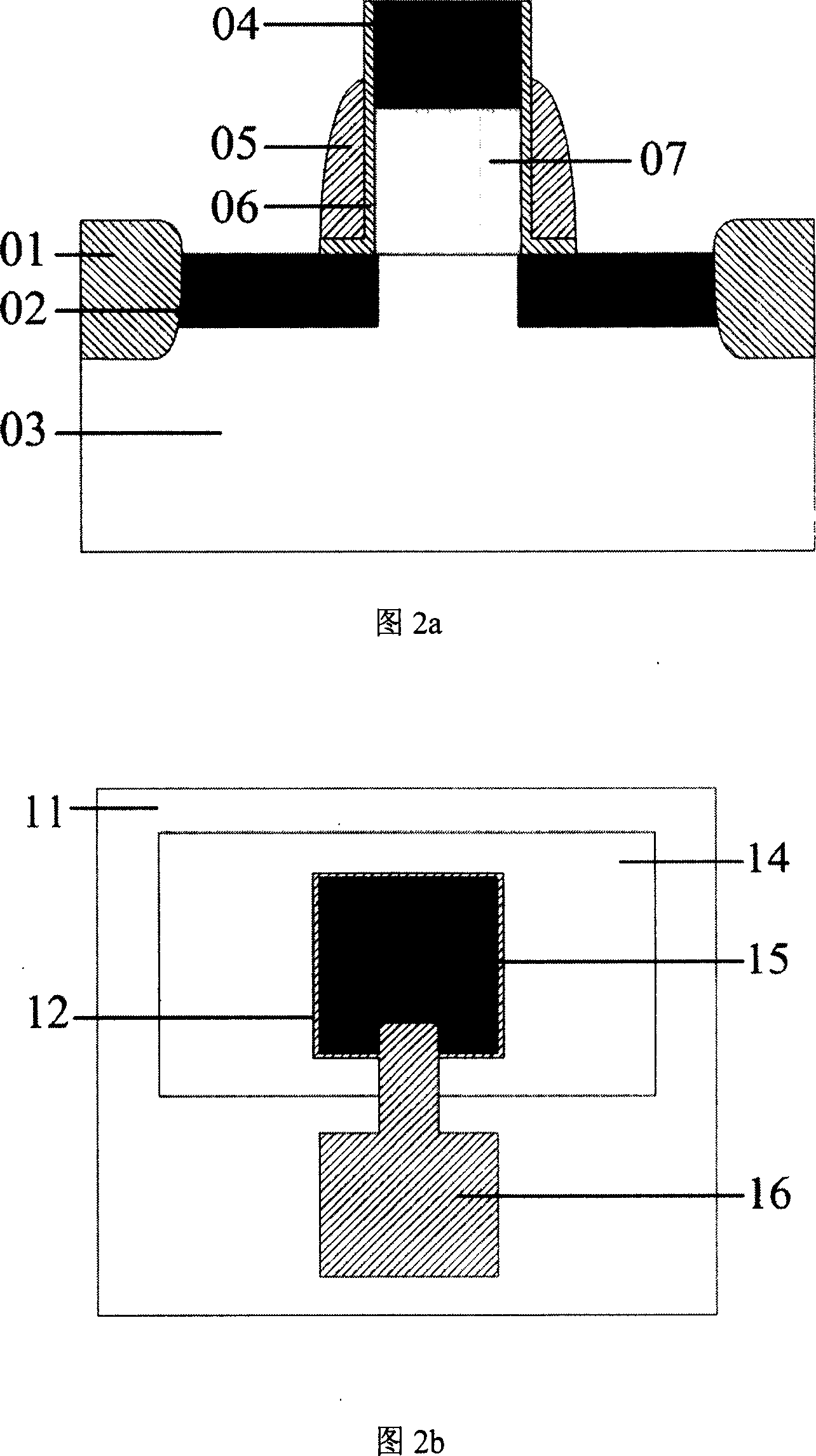
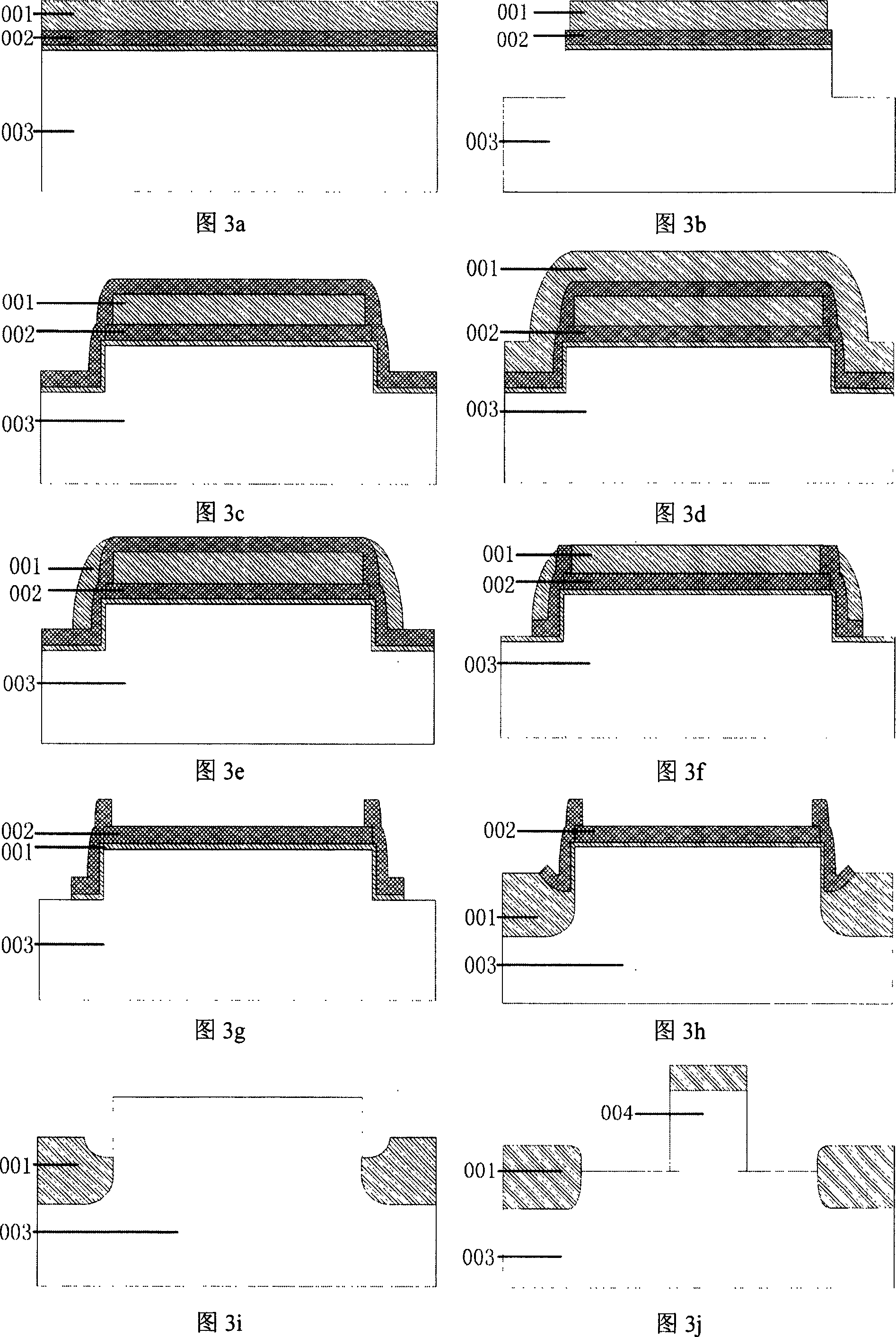
[0041] Referring to Figure 3, it is carried out on a four-inch silicon wafer, and the process steps are as follows:
[0042] 1. Thermal oxidation 500 Ȧ;
[0043] 2. LPCVD (low pressure chemical vapor deposition) 1500 Ȧ silicon nitride, the first deposition of silicon nitride;
[0044] 3. LPCVD deposition of 2000 Ȧ silicon dioxide, the first deposition of silicon dioxide;
[0045] 4. Photolithography: active area plate;
[0046] 5. RIE (reactive ion etching) silicon dioxide 2000 Ȧ;
[0047] 6. RIE etching silicon nitride 1500 Ȧ;
[0048] 7. Corrosion silicon dioxide 500 Ȧ;
[0049] 8. ICP (Inductively Coupled Plasma) etching silicon 3000 Ȧ to form a silicon platform in the active area;
[0050] 9. Degumming and cleaning;
[0051] 10. Thermal oxidation 500 Ȧ;
[0052] 11. BHF corrodes silicon oxynitride;
[0053] 12. Deposit 1500 Ȧ of silicon nitride by LPCVD, and deposit silicon nitride for the second time;
[0054] 13. Deposit 2000 Ȧ of silicon dioxide by LPCVD, and d...
PUM
 Abstract
Description
Claims
Application Information
 - R&D
- Intellectual Property
- Life Sciences
- Materials
- Tech Scout
- Unparalleled Data Quality
- Higher Quality Content
- 60% Fewer Hallucinations
Browse by: Latest US Patents, China's latest patents, Technical Efficacy Thesaurus, Application Domain, Technology Topic, Popular Technical Reports.
© 2025 PatSnap. All rights reserved.Legal|Privacy policy|Modern Slavery Act Transparency Statement|Sitemap|About US| Contact US: help@patsnap.com