MnAs nanowires and preparation method thereof

A technology of nanowire and crystal orientation, applied in the field of MnAs nanowire and its preparation

Inactive Publication Date: 2011-06-01
WUXI NANLIGONG TECH DEV
View PDF0 Cites 0 Cited by
  • Summary
  • Abstract
  • Description
  • Claims
  • Application Information

AI Technical Summary

Problems solved by technology

Therefore, although the growth of MnAs / GaAs(001) also belongs to heteroepitaxy under stress, there is no report of using this technique to obtain MnAs nanowires.

Method used


Image

  • MnAs nanowires and preparation method thereof
  • MnAs nanowires and preparation method thereof
  • MnAs nanowires and preparation method thereof

Examples


preparation example Construction

[0023] The preparation method of MnAs nano wire of the present invention comprises the following steps:

[0024] 1. First complete the various growth preparation procedures of the MBE equipment: confirm that Mn, Ga, and As sources are installed in the system; cut the GaAs (001) single crystal substrate in the ultra-clean room and adhere it to the sample stage with In; The substrate and sample stage are dehydrated and baked in the chamber, and the substrate and sample stage are baked to remove organic impurities in the buffer chamber; the growth chamber is cooled with liquid nitrogen to increase the background vacuum to 5×10 -10 Torr below.

[0025] 2. In the growth chamber, increase the growth temperature to 20°C above the deoxidation temperature of GaAs(001) single crystal, and epitaxially grow a GaAs high-temperature buffer layer with a thickness of 200nm and above to improve the interface quality of heterogeneous growth; at 450-550°C , grow MnAs nanowires, keep As in the g...

Embodiment 1

[0030] 1. First, confirm that the MBE system is equipped with at least high-purity Mn source, Ga source, and As source (purity higher than 99.999%). Complete the growth preparation procedures of the MBE equipment: cut the GaAs(001) single crystal substrate in the ultra-clean room according to the requirements and adhere it to the sample stage with molten In; put the substrate together with the sample stage into the sample entry and exit chamber, The substrate and the sample stage are dehydrated and baked; the substrate and the sample stage are transferred to the buffer chamber, and the substrate and the sample stage are baked to remove organic impurities; the growth chamber is cooled with liquid nitrogen to improve the background Vacuum to 2×10 -10 Torr below.

[0031] 2. Transfer the substrate together with the sample stage to the growth chamber, increase the growth temperature to 20°C above the deoxidation temperature of the GaAs(001) single crystal substrate, and epitaxial...

Embodiment 2

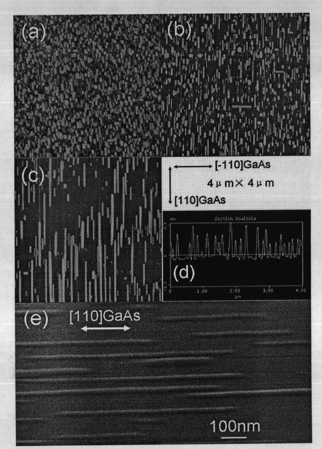
[0035] In step 2, the growth temperature was controlled to 500° C., and the rest of the steps were the same as in Example 1. The morphology of the sample is characterized by figure 1 As shown in (b), the hysteresis loop is as Figure 4 (a) shown.


PUM

PropertyMeasurementUnit
thicknessaaaaaaaaaa

Abstract

The invention discloses MnAs nanowires and a preparation method thereof. More than 90 percent of nanowires are distributed along the crystallographic direction of [110]GaAs, meet correspondence with the crystallographic direction, are epitaxially grown on a GaAs (001) monocrystalline substrate, transversely lay on the surface of GaAs (001) monocrystals and have a hexagonal close-packed crystal structure. In the invention, molecular beam epitaxy technology and equipment are adopted, GaAs (001) monocrystals are used as the substrate, a growth temperature is improved to 450 to 550 DEG C to realize S-K growth mode, a As4 to Mn flow ratio is 20 or above, the average sedimentary thickness is controlled to be between 0.4 and 3 nanometer, and thus, the epitaxial MnAs nanowires which transversely lay on GaAs(001) surface are obtained.

Description

technical field [0001] The invention belongs to MnAs nanowire technology, in particular to a MnAs nanowire and a preparation method thereof. Background technique [0002] As a typical example of crystal epitaxial growth, MnAs / GaAs heterostructure has always been the focus of research in the field of thin film crystal growth, and has potential application prospects in the fields of spin electronics such as spin injection devices, spin valves, and magnetic tunnel junctions. [0003] MnAs / GaAs heterostructures are generally grown by molecular beam epitaxy (MBE) and equipment. MBE is a technique applied to crystal thin film growth and thin film device fabrication. Through MBE equipment, not only the composition, temperature, time and other parameters of crystal growth can be adjusted, but also the orientation, lattice matching degree, stress, etc. of crystal growth can be adjusted by designing and selecting the substrate and buffer layer in the heterostructure, etc. Thus, crys...

Claims


Application Information

Patent Timeline
Patent Type & Authority Applications(China)
IPC IPC(8): C30B25/18C30B29/10C30B29/62
Inventor 徐锋陈光杜宇雷李永胜
Owner WUXI NANLIGONG TECH DEV
Why Eureka
Try Eureka