Forming method of dual damascene structure

A technology of dry etching and silicon oxide, which is applied in the fields of electrical components, semiconductor/solid-state device manufacturing, circuits, etc. It can solve the problems of inability to control the depth of trench etching, affecting the depth of trenches, and affecting the depth of through holes, etc.

Inactive Publication Date: 2013-03-27
SEMICON MFG INT (SHANGHAI) CORP +1
View PDF0 Cites 0 Cited by
  • Summary
  • Abstract
  • Description
  • Claims
  • Application Information

AI Technical Summary

Problems solved by technology

[0032] It can be seen that, in the formation method of the double damascene structure in the prior art, after the trench is formed, the bottom of the trench is etched to form a through hole. In this case, the control of the depth of the trench is It is particularly important. If the depth is not well controlled, not only the depth of the trench but also the depth of the through hole will be affected. However, in practical applications, when the trench is etched, it is difficult for the operator to observe from the surface of the wafer. To the etching depth of the trench, the etching depth of the trench cannot be precisely controlled, thereby reducing the performance of the semiconductor device

Method used


Image

  • Forming method of dual damascene structure
  • Forming method of dual damascene structure
  • Forming method of dual damascene structure

Examples


Embodiment Construction

[0059] In order to make the object, technical solution and advantages of the present invention clearer, the present invention will be further described in detail below with reference to the accompanying drawings and examples.

[0060] figure 2 For the flow chart of the formation method of a kind of double damascene structure provided by the present invention, as figure 2 As shown, the method includes:

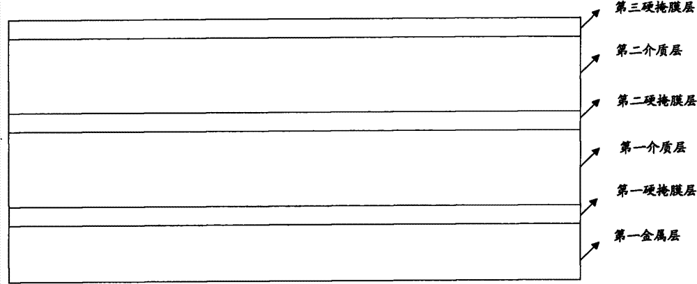
[0061] In step 201, a first hard mask layer and a first dielectric layer are sequentially deposited on the metal layer, and the first dielectric layer is etched to form via holes.

[0062] Step 202 , coating a bottom anti-reflective coating (BARC) and filling the via hole.

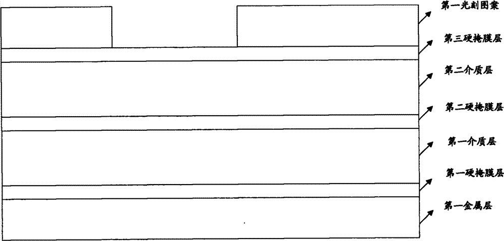
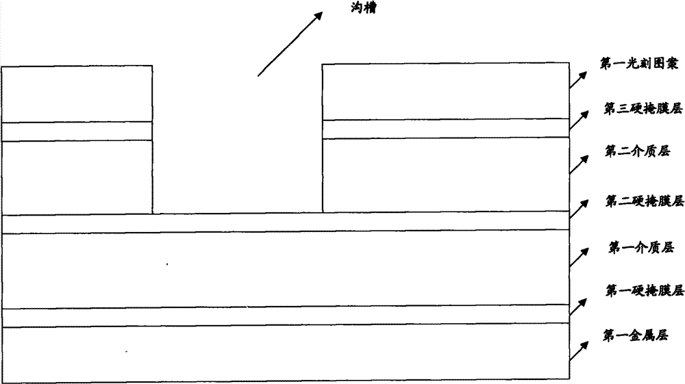
[0063] Step 203 , coating the first PR, exposing and developing the first PR to form a first photoresist pattern, wherein the width of the first PR in the first photoresist pattern is equal to the opening width of the trench.

[0064] Step 204, deposit low-temperature chemical vapor deposition (CVD) si...


PUM

PropertyMeasurementUnit
thicknessaaaaaaaaaa

Abstract

The invention provides a forming method of a dual damascene structure, comprising the following steps: coating a bottom antireflective coating (BARC) after a through hole is formed, and filling the through hole; coating a first photoresist (PR). and carrying out exposure and development on the first PR to form a first photoetching pattern, wherein the width of the first PR in the first photoetching pattern is the width of the opening of a groove; depositing low-temperature chemical vapor deposition (CVD) silicon oxide or a low temperature plasma auxiliary enhanced chemical vapor deposition (PECVD) silicon oxide on the first photoetching pattern; etching the low-temperature CVD silicon oxide or the low-temperature PECVD silicon oxide until the etched low-temperature CVD silicon oxide or the etched low-temperature PECVD silicon oxide has the same height with the first PR in the first photoetching pattern; and stripping the first photoetching pattern, so as to form a groove in the low-temperature CVD silicon oxide or the low-temperature PECVD silicon oxide. By adopting the method, the performance of a semiconductor device can be improved.

Description

technical field [0001] The invention relates to the field of semiconductor manufacturing, in particular to a method for forming a double damascene structure. Background technique [0002] With the development of semiconductor manufacturing technology, the area of ​​semiconductor chips is getting smaller and smaller, and at the same time, the number of semiconductor devices on a semiconductor chip is also increasing. In semiconductor circuits, signal transmission between semiconductor devices requires high-density metal interconnection lines. However, the large resistance and parasitic capacitance brought by these metal interconnection lines have become the main factors that limit the speed of semiconductor circuits. [0003] In traditional semiconductor technology, metal aluminum is generally used as metal interconnection lines between semiconductor devices. With the development of semiconductor technology, metal aluminum interconnection lines have been partially replaced by...

Claims


Application Information

Patent Timeline
Patent Type & Authority Patents(China)
IPC IPC(8): H01L21/768
Inventor 宁先捷
Owner SEMICON MFG INT (SHANGHAI) CORP
Why Eureka
Try Eureka