Embedded inductor structure and manufacturing method thereof

A manufacturing method and embedded technology, applied in the field of inductance, can solve the problems of low space utilization rate of vertical inductance, low utilization rate of metal wires, and difficult control of inductance value, so as to achieve performance optimization, reduce area, and ensure verticality Effect

Pending Publication Date: 2022-02-25
泉州市三安集成电路有限公司
View PDF0 Cites 0 Cited by
  • Summary
  • Abstract
  • Description
  • Claims
  • Application Information

AI Technical Summary

Problems solved by technology

Therefore, the space utilization rate of the vertical inductor is low, and the metal wire utilization rate is not high, which is not conducive to integration, and the inductance value is not easy to control

Method used


Image

  • Embedded inductor structure and manufacturing method thereof
  • Embedded inductor structure and manufacturing method thereof
  • Embedded inductor structure and manufacturing method thereof

Examples


Embodiment 1

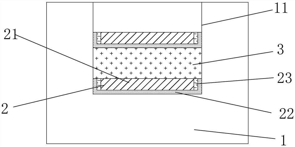
[0034] refer to figure 1 , the embedded inductor structure proposed by the embodiment of the present application includes a substrate 1 , a coil structure 2 and a second dielectric layer 3 . There is a trench 11 with a certain depth on the substrate 1, and a plurality of coil structures 2 and the second dielectric layer are stacked in the trench 11 to form an embedded inductor. Wherein, the thickness of the substrate 1 is 625-665 μm, and the material of the substrate 1 includes Si or GaAs. The depth of the trench 11 is 10 μm˜100 μm, and the sidewall of the trench 11 has a certain verticality in the substrate 1 . Specifically, the included angle between the sidewall of the ditch 11 and the bottom of the ditch 11 is 88°-92°. The coil structure 2 is arranged at intervals from the bottom of the trench 11 along the depth direction of the trench 11 to form a multi-layer coil, and a second dielectric layer 3 is arranged between two adjacent coil structures 2, and the second dielect...

Embodiment 2

[0047] refer to figure 1 , another embedded inductance structure, the difference from the first embodiment is that the adhesion layer is Si, and the metal layer is fabricated by using a self-aligned silicide (Salicide) process in step 4. Thus in case the adhesion layer is Si, the metal layer is deposited on the surface of the Si layer, and the metal layer is in contact with the surface of the Si layer. Then heat treatment is performed to form a silicide metal layer on the surface of the contact metal layer and the silicon layer. In step 5, the first dielectric layer and the Si layer on the sidewall of the trench above the silicide metal layer are removed, wherein the metal layer can be selected.

Embodiment 3

[0049] refer to Figure 4 , another embedded inductance structure, the difference from Embodiment 1 is that there is an air cavity 5 between two adjacent coil structures. Specifically, in step 6, a sacrificial material is filled between two adjacent coil structures, and the second dielectric layer is set as a sacrificial layer. In the manufacturing method, step 8 further includes: forming an air cavity 5 between adjacent upper and lower coils by opening holes and removing the sacrificial layer after the upper coil is manufactured. Sacrificial material can choose SOG.


PUM


Abstract

The invention discloses an embedded inductor structure and a manufacturing method thereof. The inductor structure comprises a substrate with a trench with a certain depth, multiple layers of coil structures spaced in the depth direction of the trench are sequentially arranged at the bottom of the trench, and each coil structure comprises a metal layer, a first dielectric layer and an adhesion layer, wherein the first dielectric layer and the adhesion layer wrap the side wall of the metal layer successively. The coil structures are attached to the side wall of the trench through adhesion layers, the adhesion layers further wrap the bottom faces of the metal layers and the bottom faces of the first dielectric layers, every two adjacent coil structures at intervals are connected through a metal connecting column, and the multiple coil structures are connected through the metal connecting columns to form an inductance structure embedded in the substrate. DRIE and a depth end point detection technology are adopted to form the trench with the vertical side wall, the number of turns of the coil structure can be adjusted according to requirements, variable control over the inductance value is achieved, and finally the purpose of optimizing the efficiency is achieved.

Description

technical field [0001] The invention relates to the field of inductance, in particular to an embedded inductance structure and a manufacturing method thereof. Background technique [0002] With the advancement of science and technology, 5G wireless communication, GPS and other technologies have emerged, and the technical requirements for high-performance radio frequency circuits and passive devices (IPD) have gradually increased. Inductor, as a commonly used electronic device in the fields of high-performance radio frequency circuits and passive devices, plays an important role in the manufacture of semiconductor circuits. [0003] The inductor is also a key part in the manufacturing process of the integrated filter (filter). The inductance value of the inductor is the main factor determining the target frequency of the filter, and the inductance value is determined by the thickness of the dielectric layer and the number of coils. The current 3D coil technology is based on ...

Claims


Application Information

Patent Timeline
Patent Type & Authority Applications(China)
IPC IPC(8): H01L49/02
CPCH01L28/10
Inventor 朱庆芳
Owner 泉州市三安集成电路有限公司
Why Eureka
Try Eureka