Producing method of semiconductor device

A technology in the direction of semiconductor and cutting, applied in the direction of semiconductor/solid-state device manufacturing, semiconductor devices, semiconductor/solid-state device parts, etc.

Inactive Publication Date: 2011-06-15
DENSO CORP
View PDF13 Cites 0 Cited by
  • Summary
  • Abstract
  • Description
  • Claims
  • Application Information

AI Technical Summary

Problems solved by technology

However, when the resin insulating layer is cut by only the second blade, cracks are generated in the cut surface of the resin insulating layer

Method used


Image

  • Producing method of semiconductor device
  • Producing method of semiconductor device
  • Producing method of semiconductor device

Examples


no. 1 example

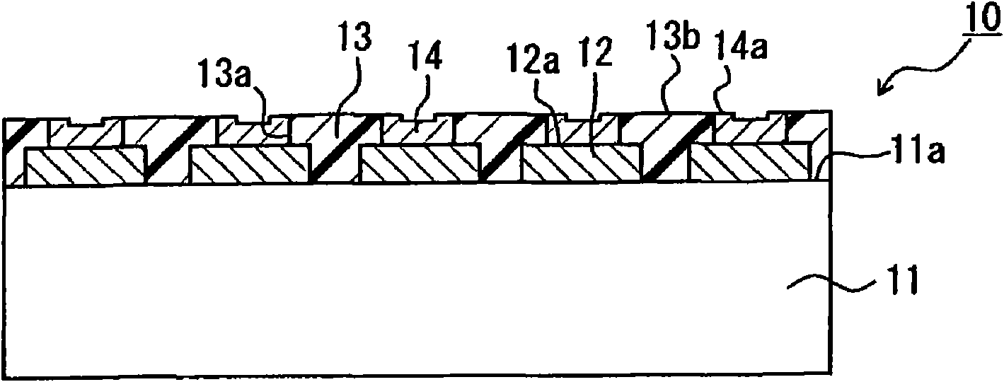
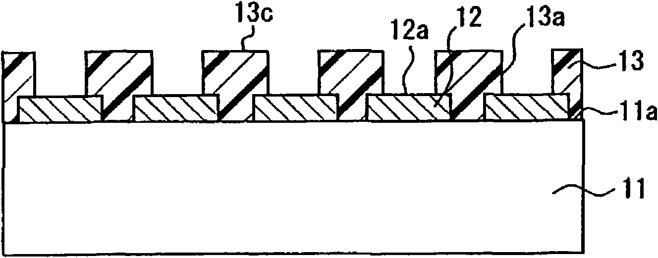
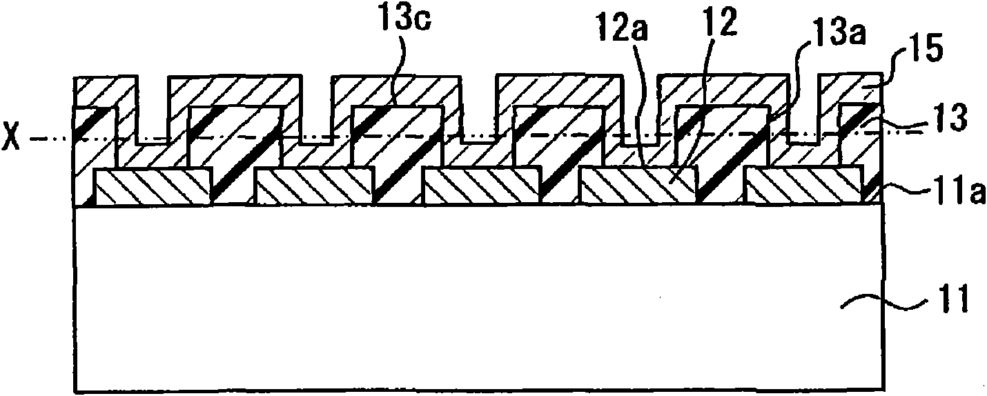
[0043] The following will refer to figure 1The structure of the semiconductor device 10 according to the first embodiment of the present invention is described. In addition, the following will refer to Figure 2A to Figure 2C A method of manufacturing the semiconductor device 10 is described. In each figure, a part of the semiconductor device 10 is enlarged and another part of the semiconductor device 10 is omitted for explanation. Figure 2B and Figure 2C The symbol X in indicates the cutting surface of the cutting tool. To make the location clear, the cutting surface X is also shown in Figure 2B middle.

[0044] In the manufacturing method of the semiconductor device 10 according to the present embodiment, (i) a part of the resin insulating layer having the surface on which the metal layer is arranged is cut in such a manner that within the resin insulating layer along the edge portion of the cutting tool and In the stress distribution of the peripheral portion of th...

no. 2 example

[0085] A method of manufacturing a semiconductor device according to a second embodiment of the present invention will be described below. In the manufacturing method according to the present embodiment, (v) a portion of the resin insulating layer 13 having the surface 13c exposed to the outside is cut by the cutting tool 30 in such a manner that along the edge of the cutting tool 30 in the resin insulating layer 13 In the stress distribution of the blade portion 30a and the peripheral portion of the blade portion 30a, the width at 90% of the maximum value is not more than 0.06 μm. To satisfy point (v), (vi) a resin insulating layer having an elongation of more than 0% and not more than 90% is used, (vii) a cutting tool whose edge portion has a radius of curvature of not more than 0.35 μm in the cutting direction is used use, and (vii) a portion of the resin insulating layer having the surface 13 c exposed to the outside is cut to a cutting thickness of not less than 0.5 μm an...


PUM


Abstract

Provided is a producing method of a semiconductor device (10). The method comprises the step of cutting a part of the resin insulating layer (13) formed on the surface (11a) of a semiconductor substrate (11) by means of a cutting tool (30). Cutting a part of the resin insulating layer (13) contains cutting the part of the resin insulating layer (13) which is provided with a metal layer (15). Cutting a part of the resin insulating layer (13) is executed in a manner that in the stress distribution of the inner resin insulating layer (13) along the edge part (30a) of the cutting tool (30) and of the periphery part of the edge part (30a), the width of 90% of the maximum value is no larger than 1.3 Mum.

Description

technical field [0001] The present invention relates to a method of manufacturing a semiconductor device, including cutting a part of a resin insulating layer formed on a surface of a semiconductor substrate using a cutting tool. Background technique [0002] Conventionally, various methods of manufacturing a semiconductor device using a cutting tool including a cutting process of removing a part of a resin insulating layer formed on the surface of a semiconductor substrate are disclosed. [0003] In the semiconductor device disclosed in Patent Document 1 (JP-A-2006-186304), a base electrode is formed on the surface of a semiconductor substrate in which an element is formed, and a protective layer made of polyimide (corresponding to resin insulating layer) is formed on the surface of the semiconductor substrate so as to cover the base electrode. The protective layer has an opening portion so that a connection portion of the base electrode connected to the metal electrode is...

Claims


Application Information

Patent Timeline
Patent Type & Authority Applications(China)
IPC IPC(8): H01L21/60H01L23/00H01L21/66
CPCH01L29/66333H01L21/304H01L2924/0002H01L2924/00
Inventor 富坂学田井明赤松和夫福田丰
Owner DENSO CORP
Why Eureka
Try Eureka