Semiconductor device and manufacturing method thereof

A manufacturing method and semiconductor technology, applied in the fields of semiconductor/solid-state device manufacturing, semiconductor devices, electric solid-state devices, etc., can solve problems such as inability to integrate optical and electrical devices, light leakage, etc.

Inactive Publication Date: 2011-06-15
SHANGHAI HUAHONG GRACE SEMICON MFG CORP
View PDF3 Cites 0 Cited by
  • Summary
  • Abstract
  • Description
  • Claims
  • Application Information

AI Technical Summary

Problems solved by technology

[0012] The purpose of the present invention is to provide a semiconductor device and its manufacturing method to solve the problem of light leakage when making optical devices in the prior art, and the problem that optical devices and electrical devices cannot be effectively integrated on the same semiconductor device

Method used


Image

  • Semiconductor device and manufacturing method thereof
  • Semiconductor device and manufacturing method thereof
  • Semiconductor device and manufacturing method thereof

Examples


Embodiment Construction

[0028] The specific implementation manners of the present invention will be described in further detail below with reference to the accompanying drawings. Throughout the description, like reference numerals refer to like parts.

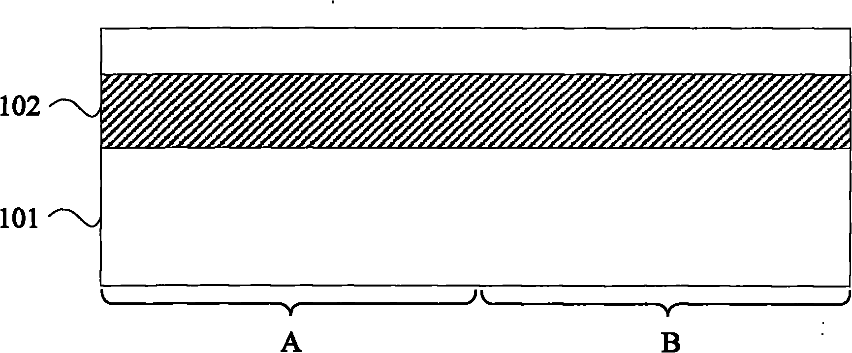
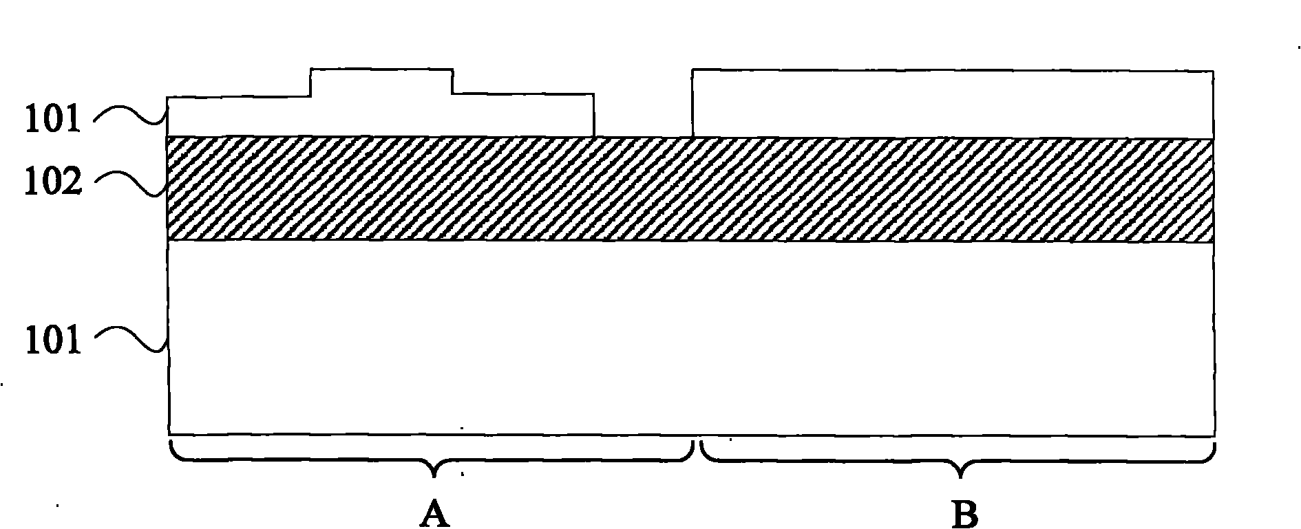
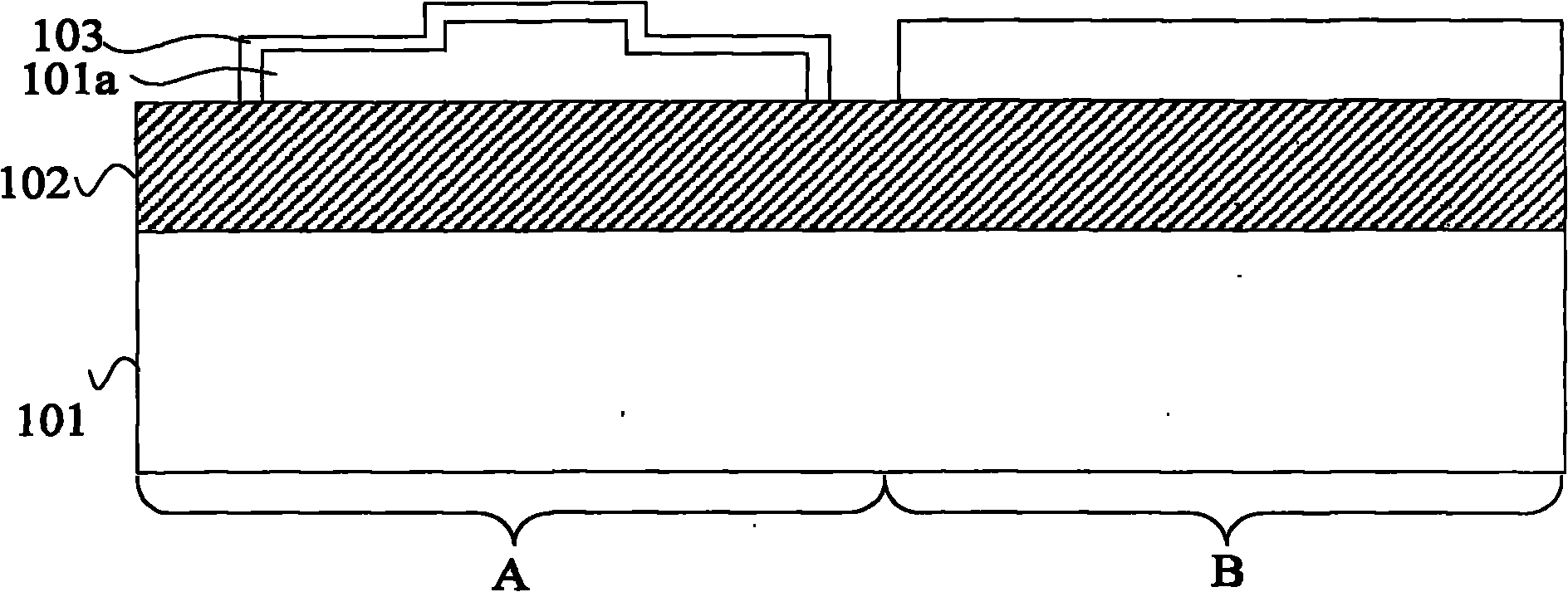
[0029] Please refer to figure 2 , which is a schematic cross-sectional view of a semiconductor device in an embodiment of the present invention. like figure 2 As shown, the semiconductor device 200 includes: a semiconductor substrate 201 having an optical device region A and an electrical device region B; an optical guide layer 201a formed by etching the optical device region A; the first oxide layer 202; the third oxide layer 204 covering the surface of the light guiding layer 201a.

[0030] In this embodiment, the material of the semiconductor substrate 201 is silicon, the material of the optical guiding layer 201a is silicon, and the material of the third oxide layer 204 is silicon dioxide. The material of the first oxide layer 202 is silicon...


PUM

PropertyMeasurementUnit
Thicknessaaaaaaaaaa

Abstract

The invention provides a semiconductor device, comprising a semiconductor substrate having an optical device area and an electrical device area, a light guide layer formed by etching the optical device area, a first oxide layer formed in the semiconductor substrate below the light guide layer, and a third oxide layer covering the surface of the light guide layer. The invention further provides a manufacturing method of the semiconductor device, which comprises the steps of: providing the semiconductor substrate, wherein the semiconductor substrate comprises the optical device area and the electrical device area; etching the optical device area to form the light guide layer; then forming a second oxide layer on the surface of the light guide layer and removing the second oxide layer by means of wet etching; forming the third oxide layer covering the surface of the light guide layer; and finally, injecting oxygen ions into the semiconductor substrate in order to form the first oxide layer in the semiconductor substrate below the light guide layer. According to the semiconductor device and the manufacturing method thereof, light leakage of the semiconductor device can be avoided, and more convenience can be brought to the integration of an optical device base plate and an electrical device base plate on the same semiconductor device.

Description

technical field [0001] The invention relates to the field of integrated circuit manufacturing, in particular to a semiconductor device and a manufacturing method thereof. Background technique [0002] At present, semiconductor devices are widely used in various modern electronic devices such as liquid crystal display devices, mobile phones, and personal digital assistants due to their high integration, low power consumption, and small size. Generally, a semiconductor device is obtained through the following manufacturing processes: first, a semiconductor device having a plurality of integrated circuits is formed; then, each integrated circuit of the semiconductor device is tested; finally, each integrated circuit is cut from the semiconductor device and Made into semiconductor devices. Currently, there are many different methods of fabricating semiconductor devices. [0003] For details, please refer to Figure 1a~1e , which is a schematic cross-sectional view of the corre...

Claims


Application Information

Patent Timeline
IPC IPC(8): H01L27/04H01L29/06H01L21/82H01L21/02
Inventor 刘巍
Owner SHANGHAI HUAHONG GRACE SEMICON MFG CORP
Why Eureka
Try Eureka