Characteristic testing system of semiconductor laser

A characteristic testing, laser technology, applied in the direction of semiconductor lasers, single semiconductor device testing, lasers, etc., can solve the problem of low test power, no polarization test, near-field nonlinear test and spatial spectrum test functions, and can not realize the test function at the same time. and other problems, to achieve the effect of accurate measurement, convenient large-scale detection application, and automatic continuous measurement.

Active Publication Date: 2011-06-29
FOCUSLIGHT TECH
View PDF4 Cites 42 Cited by
  • Summary
  • Abstract
  • Description
  • Claims
  • Application Information

AI Technical Summary

Problems solved by technology

[0006] (1) Single function: Foreign semiconductor laser test systems still do not have the functions of polarization test, near-field nonlinear test and spatial spectrum test
However, the domestic semiconductor laser test system only has the functions of LIV test and spectrum test.
[0007] (2) Low test power: Most of the semiconductor laser performance parameter test systems are mainly for testing semiconductor lasers within 100W, and the maximum test power only stays at the kilowatt level.
[0008] (3) Single LIV test mode: LIV test is mainly divided into CW (continuous wave output) mode test and QCW (quasi continuous wave output) mode test. For most test instruments, two test functions cannot be realized at the same time
[0009] (4) There are few types

Method used


Image

  • Characteristic testing system of semiconductor laser
  • Characteristic testing system of semiconductor laser
  • Characteristic testing system of semiconductor laser

Examples


Embodiment Construction

[0031] The present invention is described in further detail below in conjunction with accompanying drawing:

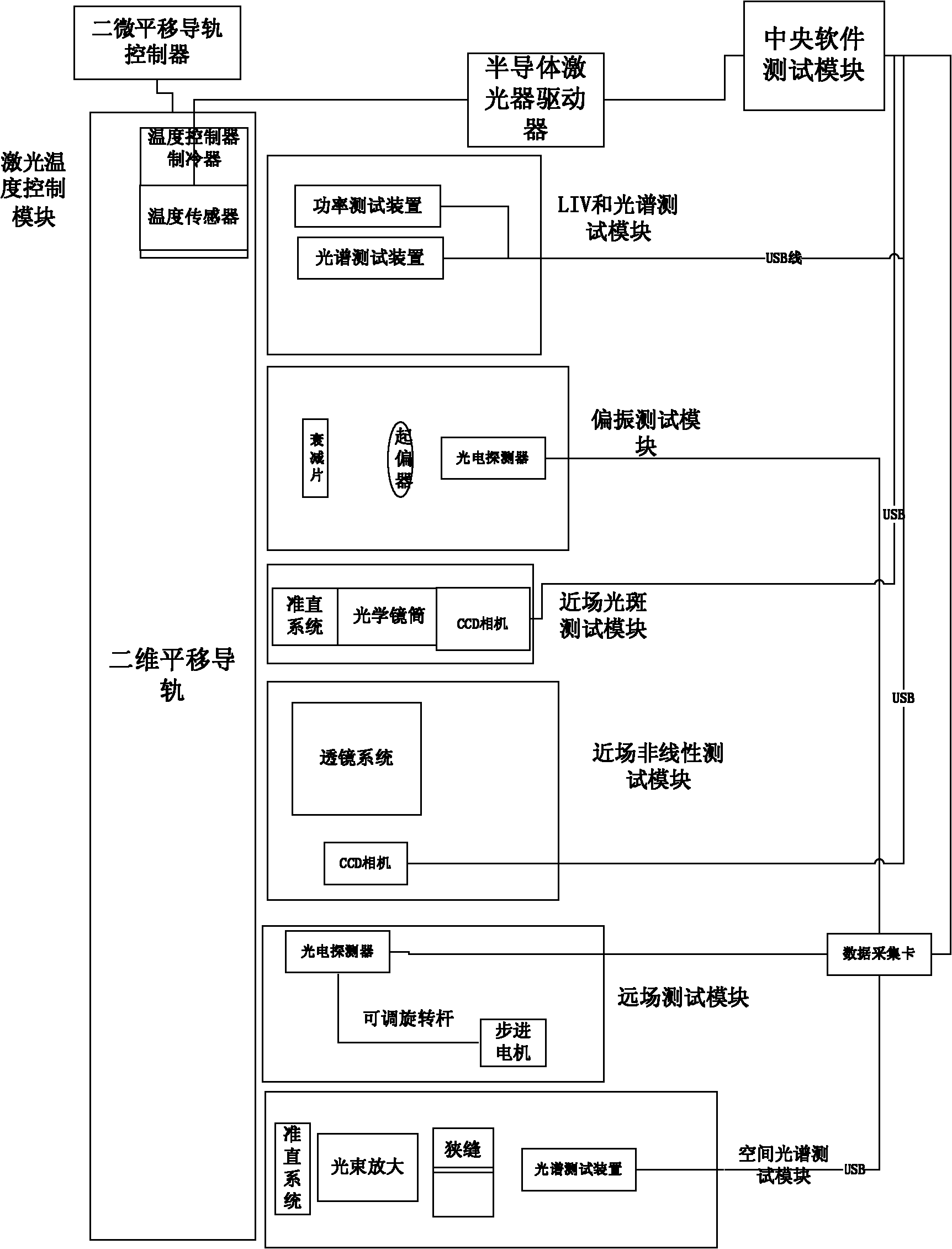
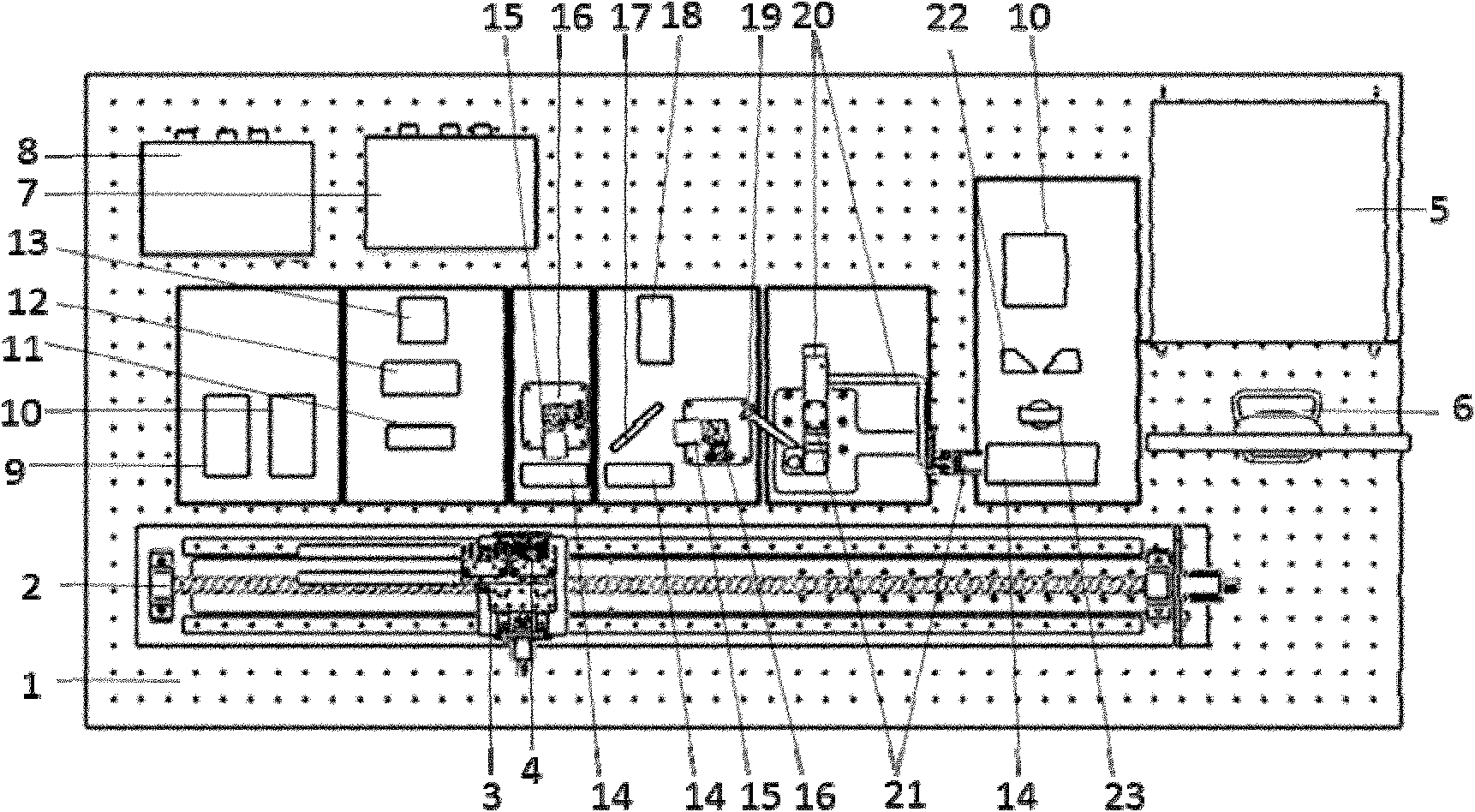
[0032] see figure 1 and figure 2 , the semiconductor laser characteristic testing system of the present invention includes an optical platform 1 and a computer system, wherein the optical platform 1 is fixedly provided with a two-dimensional translation guide rail 2, and the two-dimensional translation guide rail 2 is fixedly provided with a laser fixing seat through a slider, and the laser is fixed The base is provided with a measured laser 4, and the laser fixing base is also provided with a laser temperature control module for controlling the temperature of the measured laser 4. The side of the two-dimensional translation guide rail 2 is arranged with LIV and spectrum test modules connected to the computer system, respectively. Polarization test module, near-field spot test module, near-field nonlinear test module, far-field test module and spatial spectrum test m...


PUM


Abstract

The invention discloses a characteristic testing system of a semiconductor laser, comprising a semiconductor laser driver, three-dimensional parallel guide rails, a laser temperature control module, an LIV (power-current-voltage) and spectrum test module, a polarization test module, a near-field light spot test module, a near-field nonlinear test module, a far-field test module, a space spectrum test module and a center software processing module. Working modules can be selected according to needs simultaneously. The characteristic testing system is used for high-accuracy and automation test of the semiconductor laser, especially for a high-power semiconductor laser, so that the cost for detection and manufacture of the semiconductor laser is reduced.

Description

technical field [0001] The invention belongs to the technical field of semiconductor lasers, and relates to characteristic testing of semiconductor lasers, in particular to a semiconductor laser characteristic testing system. Background technique [0002] Semiconductor lasers have the advantages of small size, light weight, high electro-optical conversion efficiency, stable performance, high reliability and long life. And input and output equipment), film and television, manufacturing, aerospace, aviation, material processing, medical treatment, entertainment, scientific research, security protection, military, anti-terrorism, handicrafts, display and printing industries. Testing and characterization of the performance parameters of semiconductor lasers is the key to a deep understanding of the characteristics of the laser, and it is also an important basis for judging whether the laser is good or bad; only in this way can the laser be used correctly and its life extended. ...

Claims


Application Information

Patent Timeline
IPC IPC(8): G01R31/26H01S5/00
Inventor 刘兴胜吴迪张彦鑫杨凯李锋
Owner FOCUSLIGHT TECH
Why Eureka
Try Eureka