Method for performing low-temperature metal bonding on GaAs and Si

A low-temperature metal and bonding technology, applied in sustainable manufacturing/processing, electrical components, climate sustainability, etc., can solve the problems of high requirements for operators and long bonding time, and achieve high repeatability and bonding The effect of shortening the combination time and high success rate

Inactive Publication Date: 2011-06-29
INST OF SEMICONDUCTORS - CHINESE ACAD OF SCI
View PDF3 Cites 20 Cited by
  • Summary
  • Abstract
  • Description
  • Claims
  • Application Information

AI Technical Summary

Problems solved by technology

However, the first two have high requirements on experimental equipment and conditions, while the third party has low requirements on experimental equipment, but the bonding time is very long, and the requirements for operators are very high during the bonding process.

Method used


Image

  • Method for performing low-temperature metal bonding on GaAs and Si
  • Method for performing low-temperature metal bonding on GaAs and Si
  • Method for performing low-temperature metal bonding on GaAs and Si

Examples


Embodiment Construction

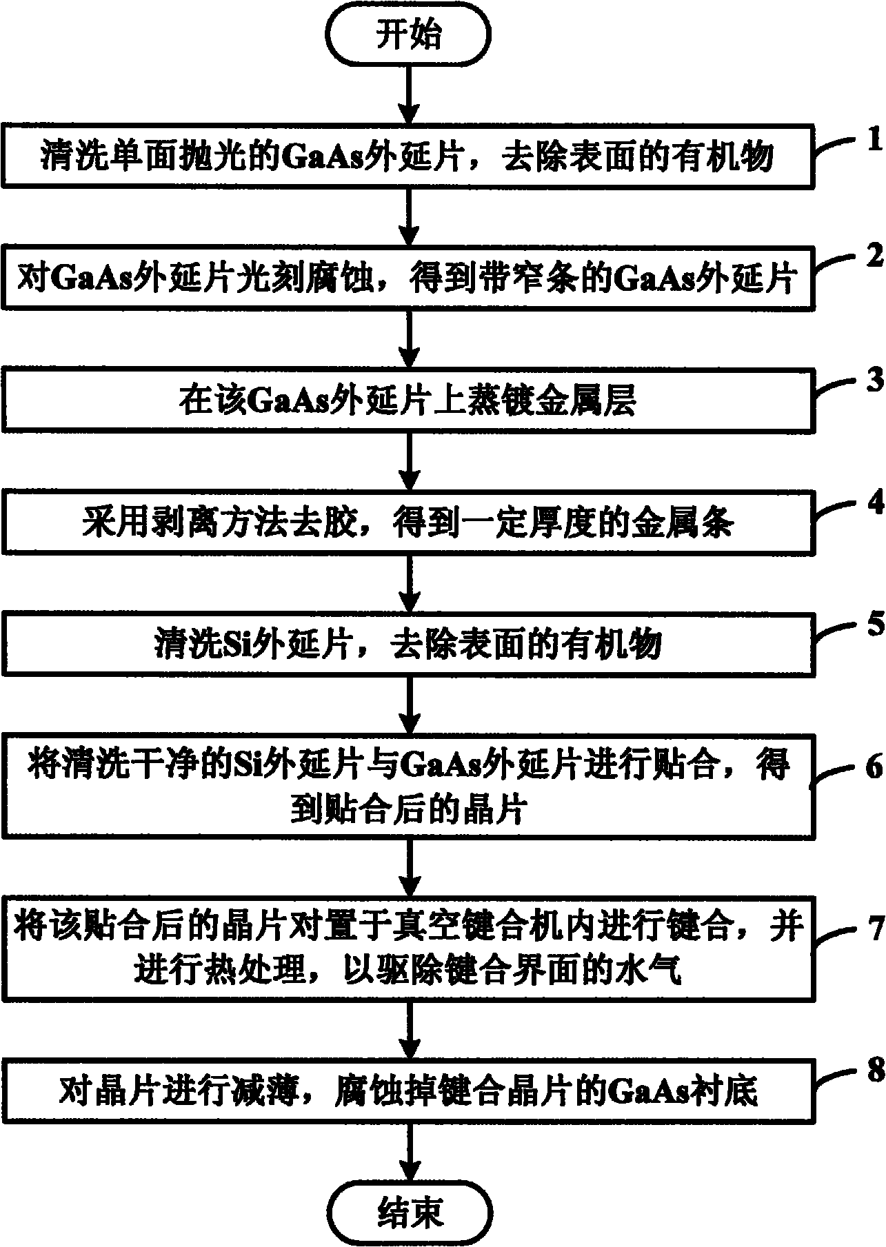
[0050] In order to make the object, technical solution and advantages of the present invention clearer, the present invention will be described in further detail below in conjunction with specific embodiments and with reference to the accompanying drawings.

[0051] The present invention is a method for low-temperature metal bonding of GaAs and Si by using a vacuum bonding machine, such as figure 1 As shown, the method includes the following steps:

[0052] Step 1: Clean the GaAs epitaxial wafer polished on one side to remove organic matter on the surface;

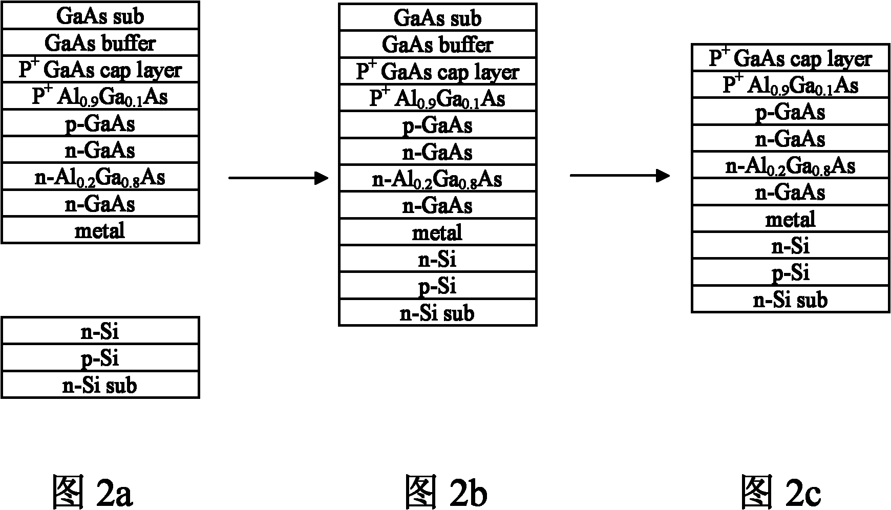
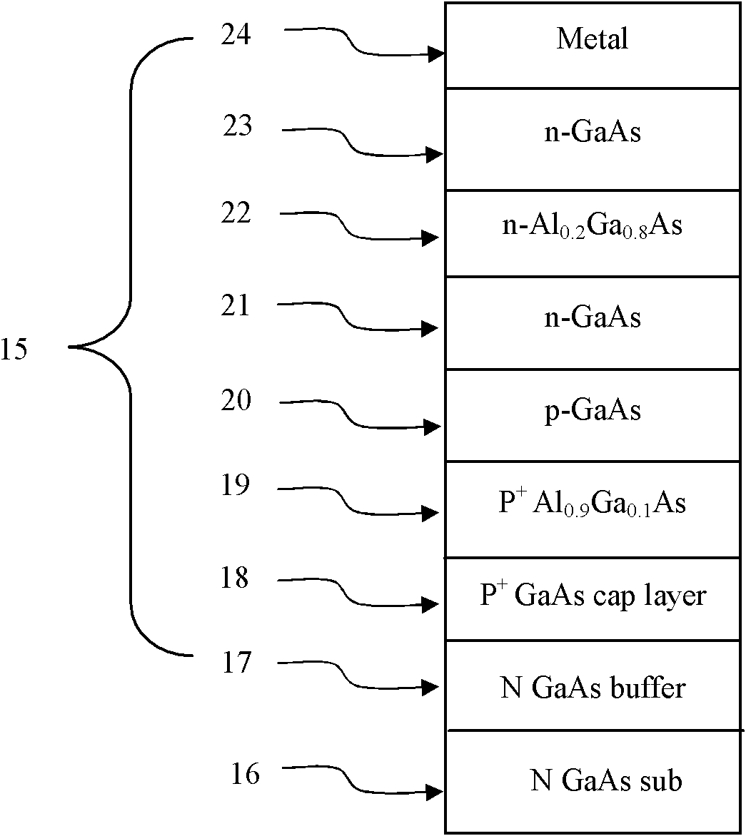
[0053] Step 2: performing photoetching on the GaAs epitaxial wafer to obtain a GaAs epitaxial wafer with narrow strips;

[0054] Step 3: Evaporating a metal layer on the GaAs epitaxial wafer;

[0055] Step 4: Use the peeling method to remove the glue to obtain a metal strip with a certain thickness;

[0056] Step 5: cleaning the Si epitaxial wafer to remove organic matter on the surface;

[0057] Step 6: Using H 2 SO ...


PUM

PropertyMeasurementUnit
thicknessaaaaaaaaaa
areaaaaaaaaaaa

Abstract

The invention discloses a method for performing low-temperature metal bonding on GaAs and Si. The method comprises the following steps of: cleaning a single-side polished GaAs epitaxial wafer to remove organic substances on the surface of the wafer; performing photoresist etching on the GaAs epitaxial wafer to obtain the GaAs epitaxial wafer with a narrow strip; performing evaporation on the GaAs epitaxial wafer to form a metal layer; removing a photoresist by a stripping method to obtain a metal strip with a certain thickness; cleaning a Si epitaxial wafer to remove organic substances on the surface of the wafer; treating the surface of the Si epitaxial wafer by using H2SO4 solution and RCAl solution and attaching the cleaned Si epitaxial wafer to the GaAs epitaxial wafer so as to obtain an attached wafer; oppositely arranging the attached wafer in a vacuum bonding machine for bonding and performing thermal treatment to remove vapor of a bonding interface; and thinning the bound wafer and corroding off the GaAs substrate of the bound wafer. By the method, the low-temperature metal bonding of the GaAs and the Si is realized; and the method can be extended to the bonding between two III-V groups (or materials such as Si, Ge and the like of an IV group).

Description

technical field [0001] The invention relates to the technical field of multi-junction solar cells in the semiconductor technology, in particular to a method for low-temperature metal bonding of GaAs and Si, and realizes the connection of any battery through bonding. Background technique [0002] Utilizing multi-junction, multi-band, or multi-level structures is one of the most realistic approaches to achieve ultrahigh-efficiency solar cells. The lattice constants of single-layer materials of multi-junction solar cells that match the solar spectrum are quite different, and the use of bonding technology to realize high-efficiency multi-junction solar cells has become a trend in the development of future solar cells. The experimental method of bonding is simple; dislocations are only localized at the interface, which breaks through the limitations of crystal orientation and lattice matching, maximizes the matching with the solar spectrum, and achieves high efficiency. The Cali...

Claims


Application Information

Patent Timeline
Patent Type & Authority Applications(China)
IPC IPC(8): H01L21/02H01L21/20H01L31/18
CPCY02P70/50
Inventor 彭红玲郑婉华石岩马绍栋
Owner INST OF SEMICONDUCTORS - CHINESE ACAD OF SCI
Why Eureka
Try Eureka