Charge trapping type nonvolatile memory and manufacturing method thereof

A non-volatile memory and charge trapping technology, which is applied in the fields of electrical solid-state devices, semiconductor/solid-state device manufacturing, circuits, etc., can solve the problems of poor device retention, reduce the probability of charge leakage, increase the erasing and writing speed, and improve The effect of maintaining performance

Inactive Publication Date: 2011-07-06
INST OF MICROELECTRONICS CHINESE ACAD OF SCI
View PDF0 Cites 2 Cited by
  • Summary
  • Abstract
  • Description
  • Claims
  • Application Information

AI Technical Summary

Problems solved by technology

[0008] Aiming at the problem that the energy band structure of the trapping layer material in the existing charge-trapping memory leads to poor device retention, the main purpose of the present invention is to provide a charge-trapping non-volatile memory and its manufacturing method to improve the performance of charge-trapping memory devices. charge retention characteristics without sacrificing other aspects of device performance

Method used


Image

  • Charge trapping type nonvolatile memory and manufacturing method thereof
  • Charge trapping type nonvolatile memory and manufacturing method thereof
  • Charge trapping type nonvolatile memory and manufacturing method thereof

Examples


Embodiment Construction

[0040] In order to make the object, technical solution and advantages of the present invention clearer, the present invention will be described in further detail below in conjunction with specific embodiments and with reference to the accompanying drawings.

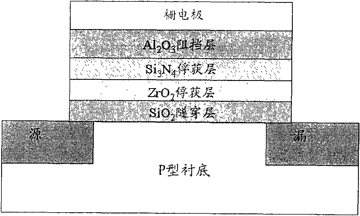
[0041] like figure 1 as shown, figure 1 The schematic diagram of the basic structure of the non-volatile memory provided by the present invention, the memory includes:

[0042] Silicon substrate 1;

[0043] heavily doped source conduction region 7 and drain conduction region 8 on silicon substrate 1;

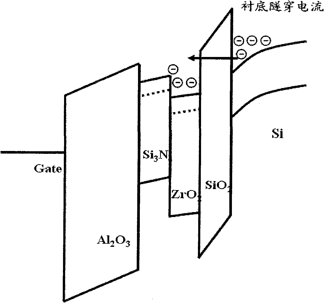
[0044] SiO is covered on the carrier channel between the source and drain conduction regions 2 A tunneling dielectric layer 2 composed of a material medium;

[0045] The first trapping layer 3 covered on the tunneling dielectric layer 2;

[0046] a second trapping layer 4 overlying the first trapping layer 3;

[0047] The ZrO composed of the first trapping layer 3 and the second trapping layer 4 2 / Si 3 N 4 High-k ...


PUM


Abstract

The invention discloses a charge trapping type nonvolatile memory and a manufacturing method thereof. The memory comprises a silicon substrate, a source conducting region and a drainage conducting region heavily doped on the silicon substrate, a tunneling dielectric layer formed by covering an SiO2 medium on a carrier channel between the source conducting region and the drainage conducting region, a first trapping layer covering on the tunneling dielectric layer, a second trapping layer covering on the first trapping layer, a control grid dielectric layer formed by high-k AI2O3 covering on a ZrO2 / Si3N4 stacked trapping layer which is formed by the first trapping layer and the second trapping layer, and a grid material layer covering on the control grid dielectric layer. The charge trapping type nonvolatile memory effectively improves the charge maintaining characteristic, is beneficial to the increasing of the memory window, improves the erasing speed, improves the memorizing characteristic comprehensively, and lays the foundation for further shrinkage of the charge trapping type nonvolatile memory.

Description

technical field [0001] The invention relates to the technical field of nanoelectronic devices and nanoprocessing, in particular to a charge-trapping nonvolatile memory and a manufacturing method thereof, which adopts a double-layer stacked trapping layer structure for energy band modulation to improve device performance. Background technique [0002] The main feature of non-volatile memory is that it can keep the stored information for a long time without power on. It has both the characteristics of read-only memory (ROM) and high access speed, and it is easy to erase and store. Rewrite, less power consumption. With the demand for large-capacity and low-power storage in multimedia applications and mobile communications, non-volatile memory, especially flash memory (Flash), occupies an increasing market share of semiconductor devices and has become a A very important type of memory. [0003] The traditional Flash memory is a silicon-based non-volatile memory using a polysil...

Claims


Application Information

Patent Timeline
Patent Type & Authority Applications(China)
IPC IPC(8): H01L29/792H01L27/115H01L21/8247
Inventor 王琴刘璟龙世兵刘明
Owner INST OF MICROELECTRONICS CHINESE ACAD OF SCI
Why Eureka
Try Eureka