Method for reducing thermal strain of surface acoustic wave device chip packaging

A surface acoustic wave device and chip packaging technology, applied in the direction of electrical components, impedance networks, etc., can solve the problems of surface acoustic wave device electrical parameter degradation, device consistency, compliance and adverse effects on reliability, etc., to achieve processing technology compatibility , Simple and compact structure, improve the effect of deterioration

Inactive Publication Date: 2013-10-09
YANGZHOU UNIV
View PDF6 Cites 1 Cited by
  • Summary
  • Abstract
  • Description
  • Claims
  • Application Information

AI Technical Summary

Problems solved by technology

[0004] The purpose of the present invention is to overcome the current surface acoustic wave device packaging thermal strain to change the geometric structure parameters of the surface acoustic wave transducer, which leads to the deterioration of the electrical parameters of the surface acoustic wave device, and then significantly affects the consistency, conformity and reliability of the device. Disadvantages of Adverse Effects

Method used


Image

  • Method for reducing thermal strain of surface acoustic wave device chip packaging
  • Method for reducing thermal strain of surface acoustic wave device chip packaging
  • Method for reducing thermal strain of surface acoustic wave device chip packaging

Examples


Embodiment 1

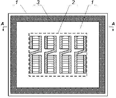
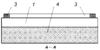
[0020] Such as figure 2 As shown, an annular metal strip 3 is fabricated by physical deposition and photolithography in the edge region of the surface of the piezoelectric single crystal substrate 1, and the annular metal strip 3, the piezoelectric single crystal substrate 1 and the packaging base 4 form a The composite structure with complementary thermal-mechanical properties reduces the distributed thermal strain generated on the surface of the piezoelectric single-crystal substrate 1 due to the thermal-mechanical mismatch between the piezoelectric single-crystal substrate material and the packaging material. The technical realization steps of the endless metal belt structure involved in this embodiment are:

[0021] (1) adopting the magnetron sputtering method to make an aluminum-copper alloy film with a copper doping ratio of 0.5% on the surface of the piezoelectric single crystal substrate 1;

[0022] (2) Manufacturing an aluminum-copper alloy annular metal belt 3 at t...

Embodiment 2

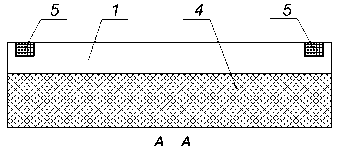
[0025] Such as image 3 As shown, an annular metal strip 5 embedded in the surface layer of the piezoelectric single crystal substrate 1 is fabricated by physical etching, physical deposition and photolithography in the edge region of the piezoelectric single crystal substrate 1, and the annular metal strip 5 is embedded in the surface layer of the piezoelectric single crystal substrate 1. Article 5. The piezoelectric single crystal substrate 1 and the packaging base 4 form a composite structure with complementary thermal-mechanical properties, which reduces the thermal-mechanical characteristics mismatch between the piezoelectric single crystal substrate material and the packaging material. Distributed thermal strain generated on the surface of the crystal substrate. The process implementation steps of the embedded annular metal strip 5 involved in this embodiment are:

[0026] (1) At the edge of the surface of the piezoelectric single crystal substrate 1, an annular groove ...


PUM


Abstract

The invention discloses a method for reducing thermal strain of surface acoustic wave device chip packaging. A set of ring-shaped structure which is synchronously manufactured with a surface acoustic wave device is manufactured in the edge area of a piezoelectric single-crystal substrate of a surface acoustic wave device chip, the ring-shaped structure is made of materials with a certain thermo-mechanical characteristic, a compound structure with complementary thermo-mechanical characteristics is formed by the ring-shaped structure, the piezoelectric single-crystal substrate and a packaging base, and the ring-shaped structure is a ring-shaped band manufactured on the surface of the piezoelectric single-crystal substrate, or a ring-shaped strip embedded into the surface layer of the piezoelectric single-crystal substrate. A thermal strain reducing structure is simple and compact, is arranged in a non-device area on the edge of the surface acoustic wave device chip, and cannot cause direct influence on parameters of a geometric structure of the surface acoustic wave device, electrical parameters of the surface acoustic wave device cannot degrade, consistency, conformance and reliability of the surface acoustic wave device can be ensured, and a manufacturing method for the thermal strain reducing structure can be compatible with a conventional processing technology of the surface acoustic wave device, and can be easily achieved with the surface acoustic wave device in a synchronous mode.

Description

technical field [0001] The invention relates to a method for controlling the thermal stress and strain of a micro-electromechanical device, in particular to a method for reducing the thermal strain of a surface acoustic wave device chip package. Background technique [0002] The surface acoustic wave device is a micro-electromechanical electronic device whose performance depends on the material parameters of the piezoelectric single crystal substrate and the geometric structure parameters of the acoustic-electric transducer fabricated on the surface of the piezoelectric single crystal substrate. During the packaging process of wave devices, due to the mismatch of thermal-mechanical properties between the piezoelectric single crystal substrate material and the packaging material, such as the thermal expansion coefficient, a distributed thermal strain will be generated on the surface of the piezoelectric single crystal substrate, thereby changing the temperature of the piezoele...

Claims


Application Information

Patent Timeline
Patent Type & Authority Applications(China)
IPC IPC(8): H03H9/64
Inventor 赵成徐威严德洋孙正亮陈磊
Owner YANGZHOU UNIV
Why Eureka
Try Eureka