Method for preparing of compound trapping layer in floating gate type nonvolatile storage

A non-volatile and memory technology, applied in semiconductor/solid-state device manufacturing, coating, nanostructure manufacturing, etc., can solve the problems of high cost, complicated manufacturing, unfavorable industrial realization, etc., to reduce manufacturing cost and simplify the process Effect

Active Publication Date: 2010-08-18
INST OF MICROELECTRONICS CHINESE ACAD OF SCI
View PDF0 Cites 0 Cited by
  • Summary
  • Abstract
  • Description
  • Claims
  • Application Information

AI Technical Summary

Problems solved by technology

However, at present, the composite trapping layer in the device is mostly made by multiple growth methods, which is complicated to make and high in cost, which is not conducive to industrial realization.

Method used


Image

  • Method for preparing of compound trapping layer in floating gate type nonvolatile storage
  • Method for preparing of compound trapping layer in floating gate type nonvolatile storage
  • Method for preparing of compound trapping layer in floating gate type nonvolatile storage

Examples


Embodiment Construction

[0030] In order to make the object, technical solution and advantages of the present invention clearer, the present invention will be described in further detail below in conjunction with specific embodiments and with reference to the accompanying drawings.

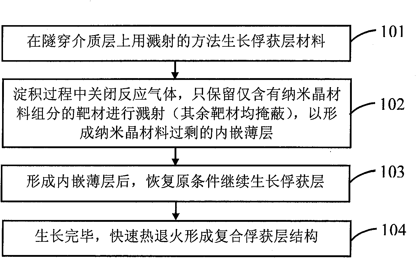
[0031] figure 1 It is a flowchart of a method for preparing a composite trapping layer in a floating gate type nonvolatile memory provided by the present invention, and the method includes:

[0032] Step 101: using a sputtering process to co-sputter various targets on the tunneling dielectric layer to deposit growth trapping layer media;

[0033] Step 102: Covering other targets during the sputtering process, sputtering a certain target material alone, forming a thin layer of embedded nanocrystals with excess nanocrystal materials in the capture layer;

[0034] Step 103: After forming the embedded nanocrystalline thin layer, restore the original process conditions (that is, the process conditions in step 1) and continue ...


PUM

PropertyMeasurementUnit
thicknessaaaaaaaaaa

Abstract

The invention discloses a method for preparing a compound trapping layer in a floating gate type nonvolatile storage, comprising the following steps of: co-sputtering a plurality of target materials on a tunneling medium layer by a sputtering process to deposit and grow a trapping layer medium; concealing other target materials and independently sputtering a certain target material in the sputtering process to form an embedded nanocrystalline thin-layer with surplus nanocrystalline materials in the trapping layer; after the embedded nanocrystalline thin-layer is formed, by recovering original process conditions to continuously grow trapping layer materials; and after the trapping layer materials are completely grown, forming a compound trapping layer structure stacked by nanocrystalline and the trapping layer through heat treatment. In the invention, the processing process of a device is compatible with the traditional CMOS (Complementary Metal-Oxide-Semiconductor Transistor) process, thereby greatly simplifying the process course, reducing the manufacturing cost and laying a foundation for the device to be trending towards practical application.

Description

technical field [0001] The invention relates to the technical field of microelectronic devices and memories, in particular to a method for preparing a composite capture layer in a floating gate type non-volatile memory by using a sputtering process. Background technique [0002] Non-volatile memory, its main feature is that it can keep the stored information for a long time without power on. It has both the characteristics of ROM and high access speed. With the demand for large-capacity and low-power storage in multimedia applications and mobile communications, the market share of non-volatile memory, especially flash memory (Flash), is becoming larger and larger, and it is also becoming more and more It has become an increasingly important type of memory. [0003] Flash memory (Flash) is the mainstream of the non-volatile memory currently on the market, but flash memory devices have excessive operating voltage, slow operating speed, insufficient durability, and the over-th...

Claims


Application Information

Patent Timeline
Patent Type & Authority Applications(China)
IPC IPC(8): H01L21/203H01L21/324H01L21/8247C23C14/34B82B3/00
Inventor 刘明刘璟王琴龙世兵
Owner INST OF MICROELECTRONICS CHINESE ACAD OF SCI
Why Eureka
Try Eureka