Shallow trench isolation structure and manufacturing method thereof

A technology of isolation structure and manufacturing method, which is applied in semiconductor/solid-state device manufacturing, electrical components, electrical solid-state devices, etc. The effect of causing standby current distribution, improving yield, and enhancing isolation performance

Active Publication Date: 2011-07-13
SEMICON MFG INT (SHANGHAI) CORP +1
View PDF8 Cites 3 Cited by
  • Summary
  • Abstract
  • Description
  • Claims
  • Application Information

AI Technical Summary

Problems solved by technology

[0007] The problem solved by the present invention is to provide a shallow trench isolation structure and its manufacturing method, which avoids poor performance of semiconductor devices caused by insufficient roundness of the liner layer in the shallow trench isolation structure and low isolation characteristics in the prior art. good question

Method used


Image

  • Shallow trench isolation structure and manufacturing method thereof
  • Shallow trench isolation structure and manufacturing method thereof
  • Shallow trench isolation structure and manufacturing method thereof

Examples


Embodiment Construction

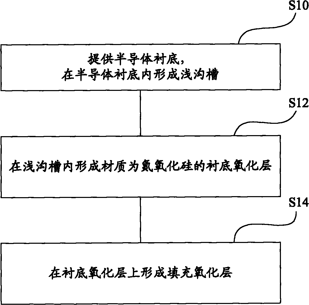
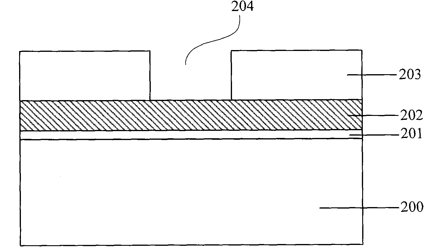
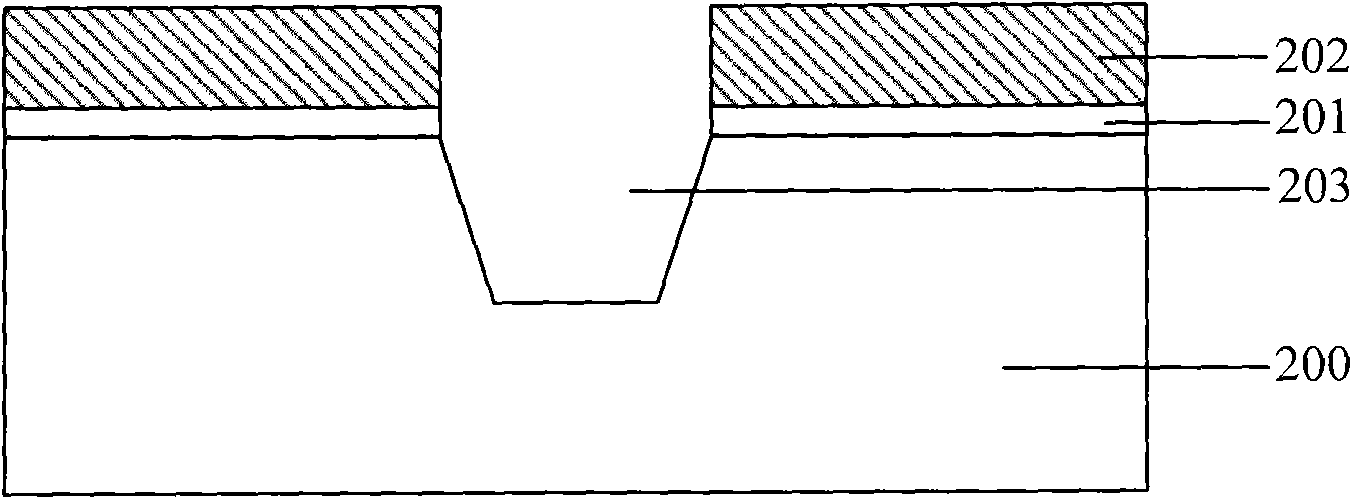
[0024] The inventors found that when making the shallow trench isolation structure, each corner of the shallow trench is sharp, and when the HDP-CVD process is used to form the filling oxide layer, because the HDP-CVD process has a certain etching ability, the plasma Bombards the liner layer formed by a thermal oxidation process such as an in-situ steam generation process (ISSG), and the isolation performance of the liner layer is weak, especially the liner layer at each corner of the shallow trench is also sharp, Therefore, the liner layer is easily destroyed under plasma bombardment, causing the filled oxide layer to directly contact the silicon substrate in the shallow trench, causing stress changes in the shallow trench, generating leakage current, and reducing the isolation characteristics of the shallow trench. , resulting in a decrease in the quality of the final semiconductor device.

[0025] Therefore, when manufacturing a semiconductor device, in order to prevent the...


PUM

PropertyMeasurementUnit
Thicknessaaaaaaaaaa

Abstract

The invention discloses a shallow trench isolation structure and a manufacturing method thereof. The manufacturing method comprises the following steps of: providing a semiconductor substrate and forming a shallow trench on the semiconductor substrate; forming a liner layer which is made of silicon oxynitride in the shallow trench; and forming a filling oxide layer for filling the shallow trench on the liner layer. According to the technical scheme, the liner layer which is made of the silicon oxynitride is formed before the shallow trench is filled, so that the smoothness of the shallow trench and a stress environment in the shallow trench can be improved, the liner layer and the semiconductor substrate below the liner layer are prevented from being damaged during implementation of subsequent process manufacturing, isolation performance of the shallow trench isolation structure is enhanced, the electrical property of a semiconductor device is improved, and the yield of a semiconductor product is further improved.

Description

technical field [0001] The invention relates to the technical field of semiconductor manufacturing, in particular to a shallow trench isolation structure and a manufacturing method thereof. Background technique [0002] In integrated circuit fabrication, shallow trench isolation structures are used to isolate devices formed on a silicon substrate from other devices. The existing technologies generally use local oxidation of silicon (LOCOS), selective polysilicon oxidation (SEPOX), recessed polysilicon spacer (RPSL) LOCOS, etc., and the LOCOS method is the most widely used one. [0003] However, there are certain problems with LOCOS isolation. That is, when the field oxide film is grown, a "bird's beak" occurs at the interface between the pad oxide film and the nitride film, or at the interface between the silicon substrate and the pad oxide film, and penetrates into the active The area reduces the reliability of the circuit. LOCOS isolation has not been further applied to...

Claims


Application Information

Patent Timeline
IPC IPC(8): H01L21/762H01L27/04
Inventor 何永根
Owner SEMICON MFG INT (SHANGHAI) CORP
Why Eureka
Try Eureka