
Manufacturing touch sensor panels using laser ablation

A touch sensor and touch surface technology, which is applied in the direction of instruments, computing, electrical digital data processing, etc., can solve the problems of technical infeasibility, high cost, thinning of touch sensor panel, etc.

Inactive Publication Date: 2016-01-20
APPLE INC
View PDF4 Cites 0 Cited by
  • Summary
  • Abstract
  • Description
  • Claims
  • Application Information

AI Technical Summary

Problems solved by technology

However, traditional touch sensor placement processes, such as photolithography and etching, which were developed for the larger mother glass sheet, are used for the smaller cover glass (cut from the mother glass sheet) after the chemical strengthening has been completed. , they are technically not feasible or too expensive
Therefore, after strengthening, it may be difficult to place the touch sensor on the cover glass using traditional placement processes
[0004] Therefore, the method of thinning the touch sensor panel has become a problem

Method used


Image

  • Manufacturing touch sensor panels using laser ablation
  • Manufacturing touch sensor panels using laser ablation
  • Manufacturing touch sensor panels using laser ablation

Examples


Embodiment Construction

[0014] In the following description of various embodiments, reference is made to the accompanying drawings which form a part hereof and which are shown by way of illustration of specific embodiments in which they can be practiced. It is to be understood that other embodiments can be utilized and structural changes can be made without departing from the scope of the various embodiments.

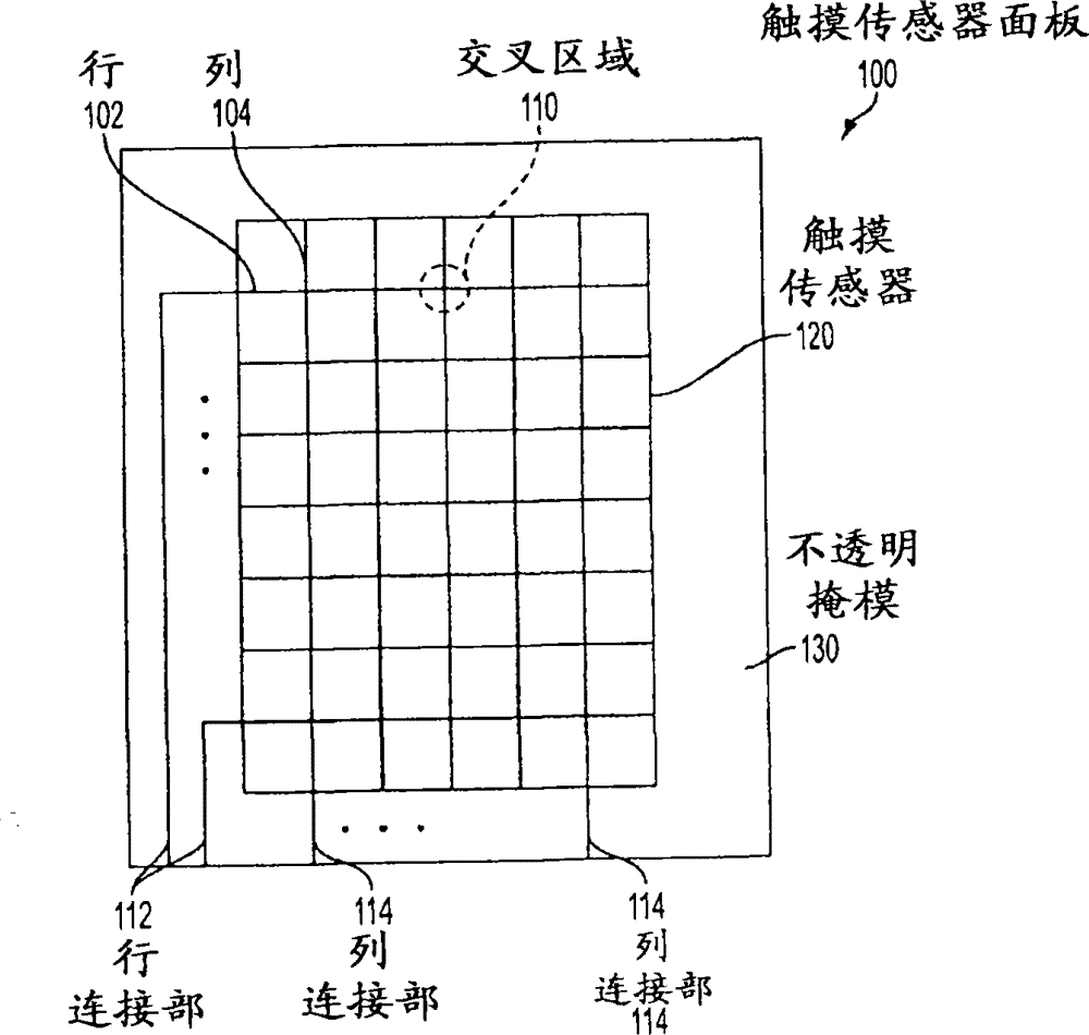
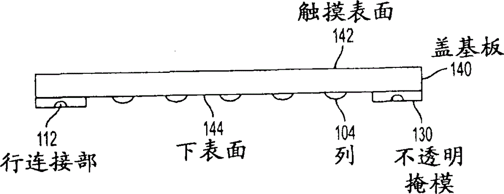
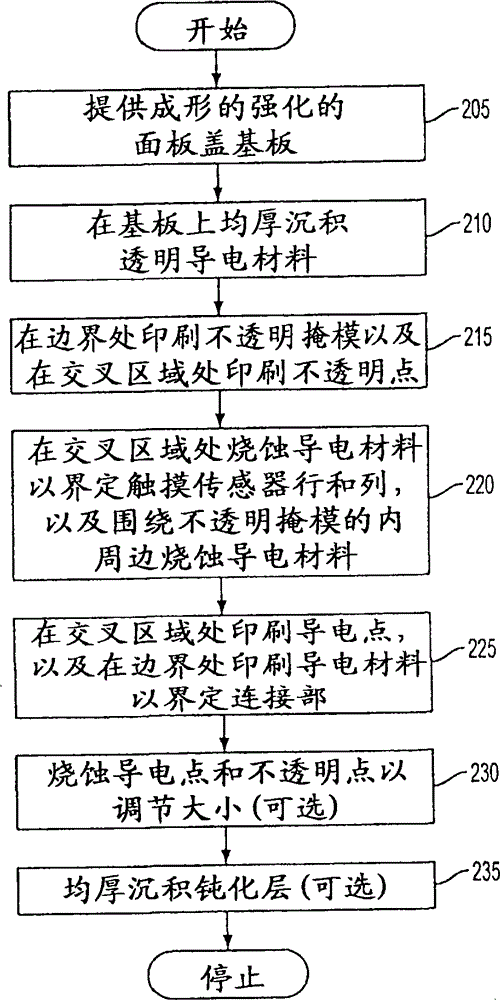
[0015] The present invention relates to the fabrication of touch sensor panels using laser ablation. The manufactured touch sensor panel may have touch sensors disposed on the lower surface of the cover substrate. The fabrication method may include: depositing a conductive layer on the substrate; depositing a dielectric material on the conductive layer; ablating the conductive layer to define different areas for the touch sensor; and depositing the conductive material on the dielectric material. Another manufacturing method may include: sputtering a conductive material on the substrate at dis...


PUM


Abstract

Fabrication of touch sensor panels using laser ablation is disclosed. The manufactured touch sensor panel may have touch sensors formed on the lower surface of its cover substrate. The fabrication method may include: depositing a conductive layer on the substrate; depositing a dielectric material on the conductive layer; ablating the conductive layer to define different areas for the touch sensor; and depositing the conductive material on the dielectric material. Another fabrication method may include: sputtering a conductive material on the substrate at discrete locations on the substrate; depositing a conductive layer over the substrate; and optionally ablating the conductive layer at the discrete locations to define a Touch different areas of the sensor. Touch sensor panels can be incorporated into mobile phones, digital media players or personal computers.

Description

technical field [0001] The present invention relates generally to touch sensor panels, and more particularly to the use of laser ablation to fabricate touch sensor panels. Background technique [0002] Touch sensor panels are increasingly being used as input devices for computing systems. Generally, a touch sensor panel may include a cover substrate (formed of glass, polymer, or the like) to input information by touch, and a sensor substrate (also formed of glass, polymer, or the like) having a touch sensor to A touch on the cover substrate is sensed. In order to manufacture thinner touch sensor panels, it is desirable to eliminate excess sensor substrate thickness. However, it is not easy to successfully provide a touch sensor panel without a sensor substrate. [0003] Elimination of the sensor substrate requires the touch sensor to preferably be located on another existing surface of the panel. A preferred surface is the lid substrate. However, lid substrates are not ...

Claims


Application Information

Patent Timeline
Patent Type & Authority Patents(China)
IPC IPC(8): G06F3/041
CPCG06F2203/04111G06F3/0443G06F3/0446Y10T29/435G06F3/041
Inventor J·A·哈勒
Owner APPLE INC
Features
  • Generate Ideas
  • Intellectual Property
  • Life Sciences
  • Materials
  • Tech Scout
  • Unparalleled Data Quality
  • Higher Quality Content
  • 60% Fewer Hallucinations
Learn More