BSIM4 stress model applied to MOSFET electrical simulation

A stress model and simulation technology, applied in special data processing applications, electrical digital data processing, instruments, etc.

Active Publication Date: 2011-08-03
EAST CHINA NORMAL UNIV +1
View PDF3 Cites 24 Cited by
  • Summary
  • Abstract
  • Description
  • Claims
  • Application Information

AI Technical Summary

Problems solved by technology

But at the same time, there are some unintentional stresses, most of which are related to the layout of the layout, and the source of stress related to the layout is mainly the LPE (Layout proximity Effect) effect

Method used


Image

  • BSIM4 stress model applied to MOSFET electrical simulation
  • BSIM4 stress model applied to MOSFET electrical simulation
  • BSIM4 stress model applied to MOSFET electrical simulation

Examples


Embodiment Construction

[0046] The present invention will be further elaborated below in conjunction with the accompanying drawings and examples. The following examples do not limit the invention. Without departing from the spirit and scope of the inventive concept, changes and advantages that can be imagined by those skilled in the art are all included in the present invention.

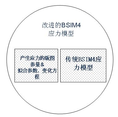
[0047] The present invention provides a BSIM4 stress model applied to MOSFET electrical simulation, which is a layout-related BSIM4 stress model of 22nm-130nm standard process MOSFET, which has clear physical meaning and high accuracy, and can be used for different layouts under certain bias conditions Parametric MOSFET electrical characteristics are simulated.

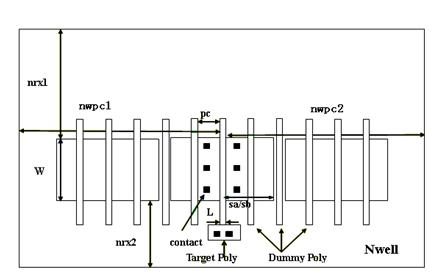
[0048] The following will further describe in detail how to apply the layout-related BSIM4 stress model of the 40nm standard process MOSFET of the present invention with examples.

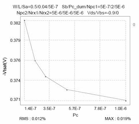
[0049] Based on the standard BSIM4 model, the present invention introduces the st...


PUM


Abstract

The invention relates to a Berkeley short-channel insulated gate field effect transistor (IGFET) model 4 (BSIM4) stress model applied to metal-oxide-semiconductor field effect transistor (MOSFET) electrical simulation. On the basis of a standard BSIM4 model, layout parameters capable of generating stress are used as entity parameters, wherein a value of each layout parameter is a designed layout size, and the layout parameters comprise space between adjacent polysilicon (PC), the number of dummy PC, space between shallow trench isolation (STI) and the PC, space between Nwell and the PC and space between the boundaries of the Nwell and oxides (OD); layout parameters and influence coefficients are added, wherein the layout parameters are fitting parameters for expressing an effective value of each layout parameter, and the influence coefficients are fitting parameters for expressing the influence degree of each layout parameter on basic parameters Vth0 and mu 0 of the BSIM4 model; and amethod for determining the change characteristics of saturated threshold voltage Vtsat and saturated drain current Idsat of a transistor according to the layout parameters is provided, namely the influence of the layout parameters on the threshold voltage Vth0 of a long-channel device under zero substrate bias and mobility mu 0 under a low electric field is considered on the basis of the standardBSIM4 model; and the threshold voltage Vth0 of the long-channel device under the zero substrate bias and the mobility mu 0 under the low electric field are defined again.

Description

technical field [0001] The invention belongs to the field of integrated circuits, in particular to a BSIM4 stress model applied to MOSFET electrical simulation. Background technique [0002] As the feature size of semiconductor devices decreases and enters the nanometer level, the layout area continues to shrink, which introduces stress to the device and affects its electrical performance, causing the threshold voltage of the MOSFET to drift, and the mobility of the carriers. device output characteristics. For designers in the field of integrated circuit design, it is very necessary to consider the influence of stress on circuit performance during design. Therefore, a SPICE model with accurate stress model parameters can predict the electrical characteristics of devices under different stress conditions in the same way that ordinary SPICE models predict the electrical characteristics of devices for integrated circuit design engineers. By introducing stress parameters into ...

Claims


Application Information

Patent Timeline
Patent Type & Authority Applications(China)
IPC IPC(8): G06F17/50
Inventor 石艳玲李曦汪明娟任铮胡少坚陈寿面彭兴伟唐逸
Owner EAST CHINA NORMAL UNIV
Why Eureka
Try Eureka