Supercharge Your Innovation With Domain-Expert AI Agents!

III-nitride compound semiconductor element and manufacturing method thereof

A manufacturing method and nitride technology, which is applied in the manufacture of semiconductor/solid-state devices, semiconductor devices, electrical components, etc., can solve the problem of peeling off the insulating protective film, inability to effectively protect the semiconductor element, and poor adhesion between the metal layer and the insulating protective film and other problems, to achieve the effect of improving reliability, high tightness, and improving reliability

Inactive Publication Date: 2011-08-03
TOYODA GOSEI CO LTD
View PDF10 Cites 2 Cited by
  • Summary
  • Abstract
  • Description
  • Claims
  • Application Information

AI Technical Summary

Problems solved by technology

However, there is a problem that the adhesion between the metal layer and the insulating protective film is poor, the insulating protective film is easily peeled off, and the semiconductor element cannot be reliably protected.

Method used


Image

  • III-nitride compound semiconductor element and manufacturing method thereof
  • III-nitride compound semiconductor element and manufacturing method thereof
  • III-nitride compound semiconductor element and manufacturing method thereof

Examples


Embodiment 1

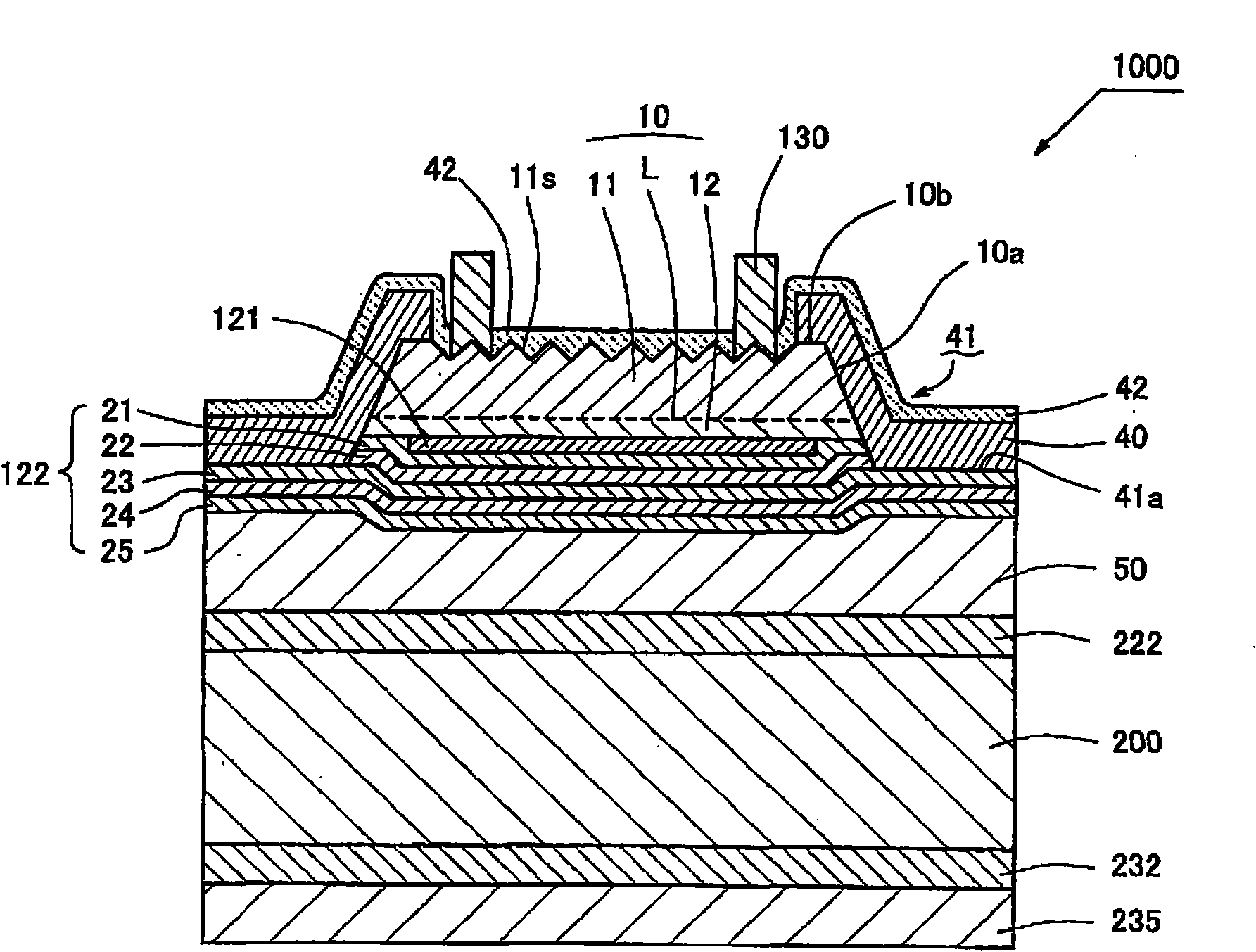
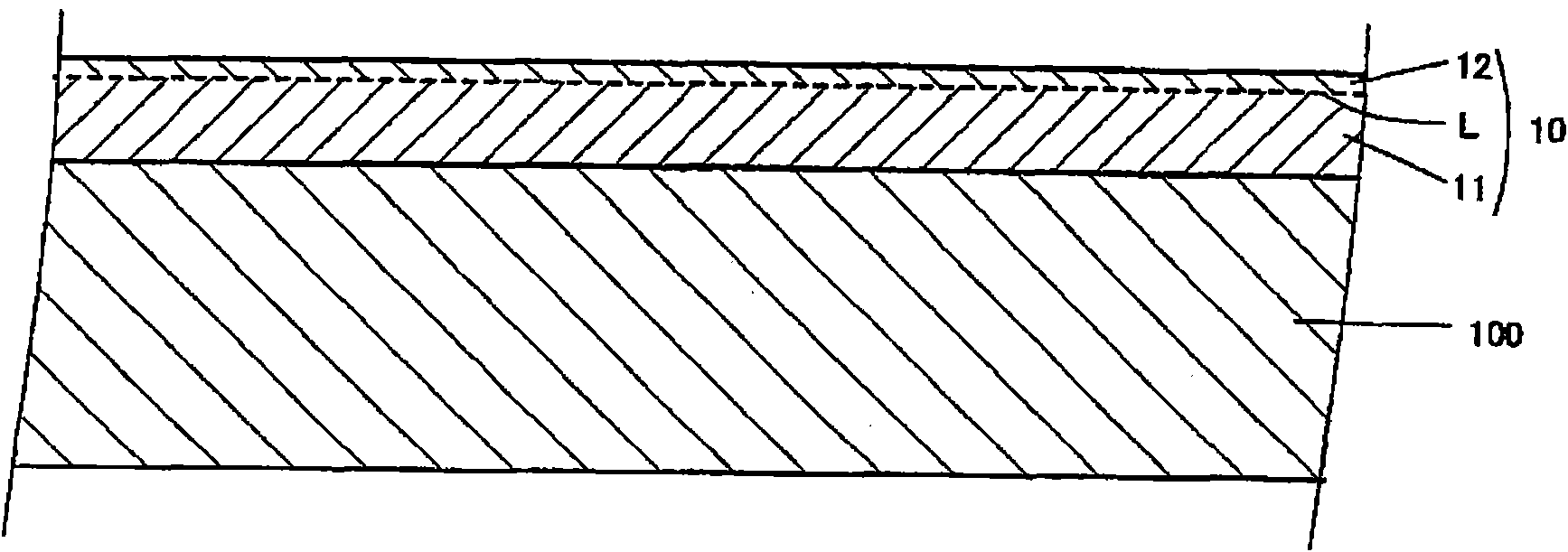
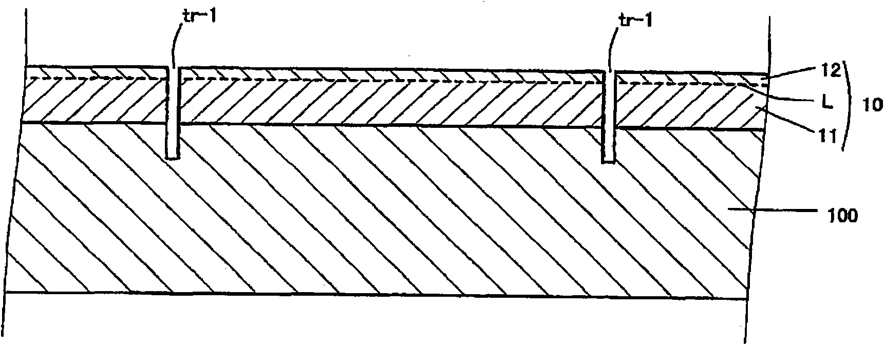
[0039] figure 1 is a cross-sectional view showing the structure of a III-nitride compound semiconductor element (blue LED) 1000 obtained by a manufacturing method according to a specific example of the present invention. figure 1 The III-nitride compound semiconductor device (blue LED) 1000 has the following stacked structure: on the surface of the p-type silicon substrate, that is, the conductive support substrate 200, multiple metals are laminated from the side closer to the support substrate 200. The second conductive layer 222 composed of laminated layers, the solder layer (solder layer) 50 as a low melting point alloy layer, the first conductive layer 122 composed of laminated layers of various metals, the p-contact electrode 121, mainly p-type a single-layer or multi-layer p-type layer 12 of a Group III nitride compound semiconductor layer, a light-emitting layer L, a single-layer or multi-layer n-type layer 11 of a mainly n-type Group III nitride compound semiconductor ...


PUM

PropertyMeasurementUnit
thicknessaaaaaaaaaa
thicknessaaaaaaaaaa

Abstract

The invention provides a manufacturing method of a III-nitride compound semiconductor element, which comprises the following steps: growing an epitaxial growth layer by crystallization on a crystallizing growth substrate, engaging a final growth layer of the epitaxial growth layer with a supporting substrate by a metal layer, removing the crystallizing growth substrate, using a substrate layer of a initial growth layer of the epitaxial growth layer as a top layer of the epitaxial growth layer on the supporting substrate. A first layer formed from metal with nitrogen reactivity, a second layer formed from metal with resistance to chlorine plasma etching and with wet etchability, and a third layer formed from metal with nitrogen reactivity and resistance to wet etching are formed at a side of the final growth layer. An element separating trough is formed by perfoming etching on the substrate layer of the semiconductor element with chlorine plasma to expose the surface of the second layer. The second layer exposed on the bottom surface of the element separating trough is removed by wet etching so as to expose the third layer on the bottom surface of the element separating trough, and the element separating trough is covered with an insulating protective film.

Description

technical field [0001] The present invention relates to the improvement of the tight bonding of the insulating protective film in a semiconductor element manufactured by forming a group III nitride compound semiconductor layer on a growth substrate, bonding the uppermost layer to a conductive support substrate, and removing the growth substrate. Semiconductor device and its manufacturing method. Background technique [0002] Conventionally, there is known a method of epitaxially growing a Group III nitride compound semiconductor layer on a growth substrate, then bonding the final growth layer of the epitaxial growth layer to a conductive support substrate, and removing the growth substrate. A sapphire substrate or the like is used as the growth substrate. In addition, a metal such as copper, a conductive silicon substrate, or the like is used as the supporting substrate. As a method of removing the growth substrate from the epitaxial growth layer, there are laser separatio...

Claims


Application Information

Patent Timeline
Patent Type & Authority Applications(China)
IPC IPC(8): H01L33/00H01L21/20H01L21/02H01L33/32H01L29/20
Inventor 上村俊也荒添直棋
Owner TOYODA GOSEI CO LTD
Features
  • R&D
  • Intellectual Property
  • Life Sciences
  • Materials
  • Tech Scout
  • Unparalleled Data Quality
  • Higher Quality Content
  • 60% Fewer Hallucinations
Learn More