Manufacturing methods for dual damascene process and integrated circuit

A manufacturing method and process technology, applied in the field of integrated circuit manufacturing using the double damascene process manufacturing method, can solve the problem of oblique facets that cannot completely solve the thickness difference, cannot protect the top of both sides of the through hole, and reduce the thickness of the filling material and other problems, to achieve the effect of subtracting the spin-coating filling material and etching back process steps, improving the shape of the beveled facet, and improving the stability

Inactive Publication Date: 2011-08-03
SHANGHAI INTEGRATED CIRCUIT RES & DEV CENT
View PDF2 Cites 4 Cited by
  • Summary
  • Abstract
  • Description
  • Claims
  • Application Information

AI Technical Summary

Problems solved by technology

The difficulty encountered in this mainstream approach is that after the through-hole etching, the area where the through-hole area is located needs to be filled with anti-etching materials to achieve optimal surface flatness. There are two main methods, one is direct spin coating filling Material, the disadvantage of this method is that after spin coating, the thickness of the filling material in the via area is always smaller than that of the non-via area, and the filling material where the via is located will form a pit shape, which will cause etching In the process, after the anti-reflection layer is etched, the filling material in the via hole area drops, and cannot protect the tops on both sides of the via hole, so that the sloped facets formed on the top of the via hole ( figure 1 It shows the d

Method used


Image

  • Manufacturing methods for dual damascene process and integrated circuit
  • Manufacturing methods for dual damascene process and integrated circuit
  • Manufacturing methods for dual damascene process and integrated circuit

Examples


Embodiment Construction

[0029] In order to make the content of the present invention clearer and easier to understand, the content of the present invention will be described in detail below in conjunction with specific embodiments and accompanying drawings.

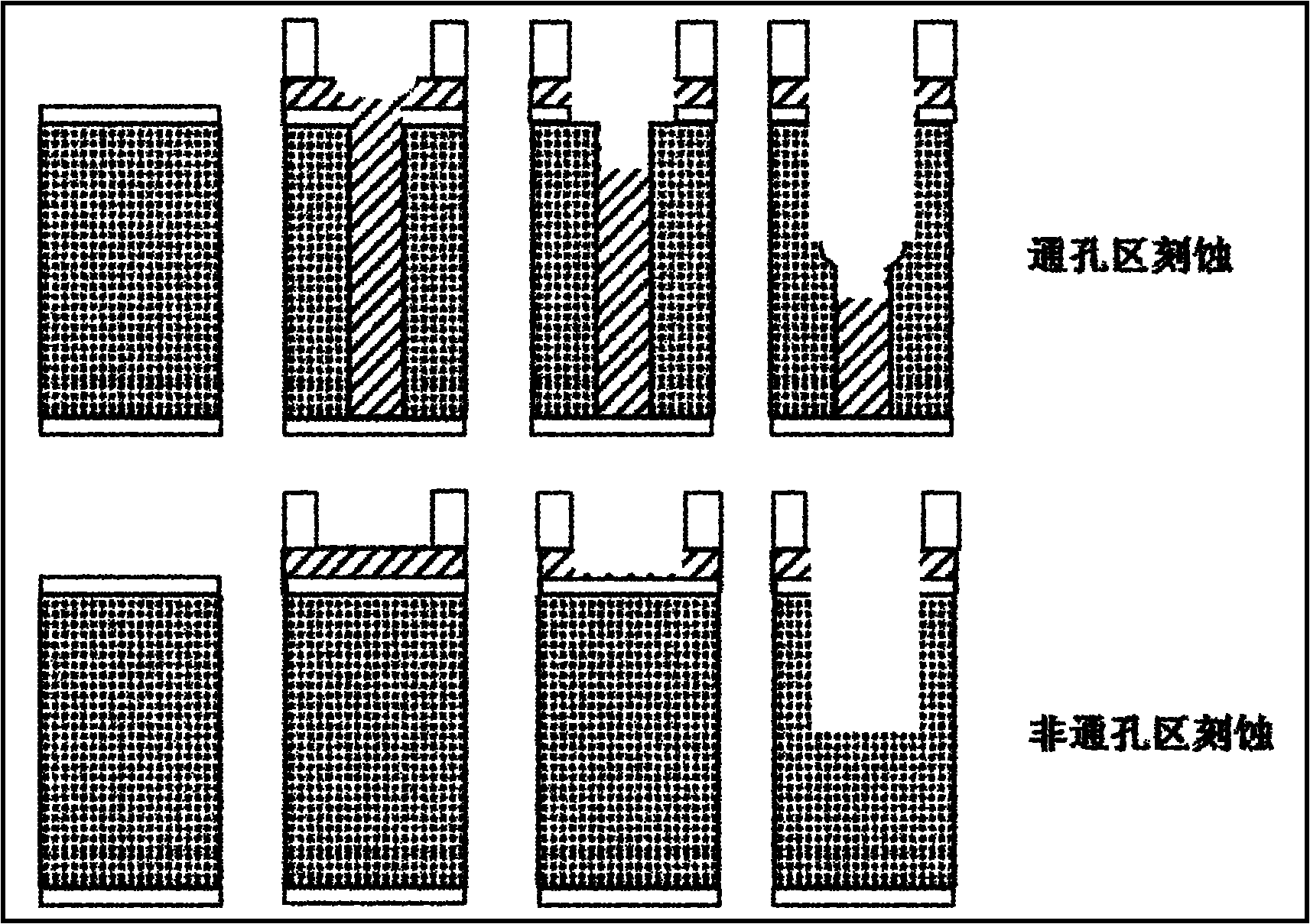
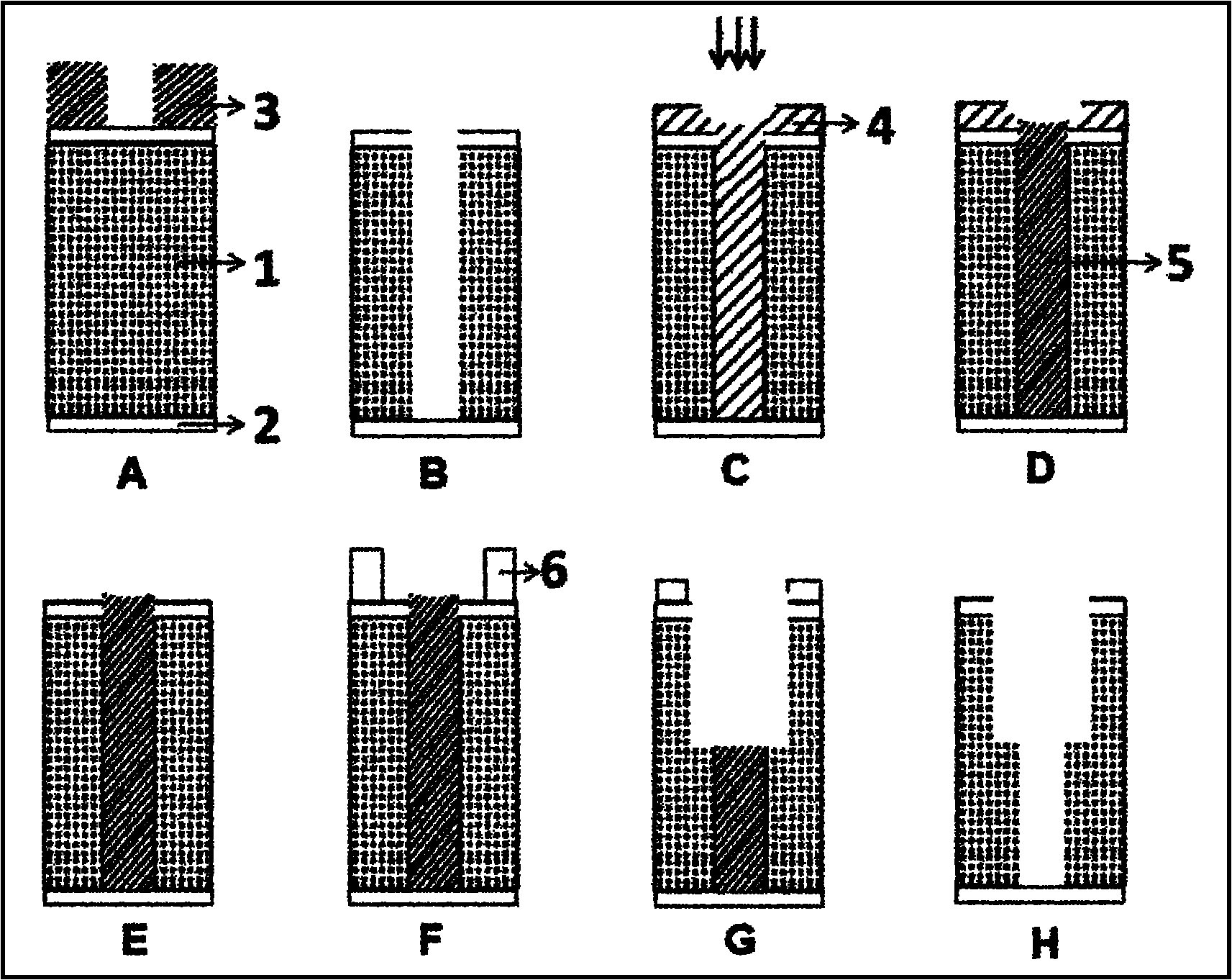
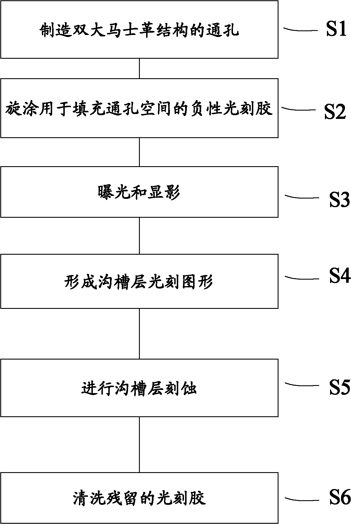
[0030] figure 2 is a schematic illustration of an embodiment of the invention; and image 3 It is a flowchart of an embodiment of the present invention. Therefore, we will now combine figure 2 and image 3 Preferred embodiments of the present invention will be described.

[0031] First, in image 3 In step S1, the via hole of the double damascene structure is fabricated. Specifically, see figure 2 A in and figure 2 In B, first make and complete the photolithography and etching of the via layer of the double damascene structure, including the dual damascene dielectric layer 1 and the bottom etch stop layer 2 and the photolithographic pattern 3 of the via layer. It can then be further stripped and cleaned. Those skilled in the art can...


PUM

PropertyMeasurementUnit
Thicknessaaaaaaaaaa
Thicknessaaaaaaaaaa

Abstract

The invention provides manufacturing methods for a dual damascene process and an integrated circuit. The manufacturing method for the dual damascene process comprises: a through hole forming step, in which a through hole is formed by a photomask; a through hole filling step, in which the through hole formed in the through hole forming step is filled by a negative photoresist; a through hole area exposing and developing step, in which a filled through hole area is exposed and developed by the photomask which is the same as a through hole layer after the through hole filling step; and a groove forming step, in which a groove is formed after the through hole filling step. According to the methods, a space of the etched through hole is filled by the negative photoresist with good hole filling performance, so that good filling of the space of the through hole is guaranteed, the good flatness of a surface of a silicon wafer is recovered, and the appearance of an oblique etched face of the etched groove is improved.

Description

technical field [0001] The invention relates to the technical field of integrated circuit manufacturing technology, in particular to an improved double damascene manufacturing method and an integrated circuit manufacturing method using the double damascene manufacturing method. Background technique [0002] With the continuous improvement of integrated circuit manufacturing technology, the volume of semiconductor devices is becoming smaller and smaller, making the resistance and parasitic capacitance between metals also increasing. For microprocessors, the limitation of chip speed is mainly caused by the resistance and parasitic capacitance in the plating layer. As a result, problems such as resistance-capacitance time delay, mutual interference between signals and energy loss have become increasingly prominent. [0003] In order to solve the problem of resistance-capacitance time delay, in terms of resistance, in the past 30 years, the semiconductor industry has used alumin...

Claims


Application Information

Patent Timeline
IPC IPC(8): H01L21/768H01L21/311G03F7/00
Inventor 袁伟
Owner SHANGHAI INTEGRATED CIRCUIT RES & DEV CENT
Why Eureka
Try Eureka